


Request Quote
(Ships tomorrow)
FDFM2P110 Equivalent & Substitute Parts
Part Overview
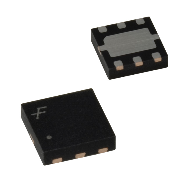
The FDFM2P110 is a P-Channel MOSFET manufactured by onsemi, rated for 20V drain-to-source voltage with 3.5A continuous drain current at 25°C. This device features the PowerTrench® series technology in a 6-WDFN Exposed Pad surface mount package (3x3mm footprint). The FDFM2P110 is classified as obsolete, necessitating identification of active equivalent parts for new designs and ongoing production requirements. Substitute parts must maintain electrical compatibility across voltage ratings, current handling, gate charge characteristics, and thermal performance while meeting modern compliance standards.
Substiute Parts
Key Parameters
| Parameter | Value | Unit |
|---|---|---|
| FET Type | P-Channel | — |
| Drain to Source Voltage (Vdss) | 20 | V |
| Current - Continuous Drain (Id) @ 25°C | 3.5 | A |
| Rds On (Max) @ Id, Vgs | 140 mOhm @ 3.5A, 4.5V | — |
| Vgs(th) (Max) @ Id | 1.5 | V @ 250µA |
| Gate Charge (Qg) (Max) @ Vgs | 4 | nC @ 4.5V |
| Power Dissipation (Max) | 2 | W |
| Operating Temperature Range | -55 to 150 | °C (TJ) |
| Package / Case | 6-WDFN Exposed Pad | 3x3mm |
| RoHS Status | ROHS3 Compliant | — |
Substitute Part Grouping Explanation
Substitute parts for the FDFM2P110 are identified based on strict electrical and mechanical compatibility criteria. The following parameters define acceptable substitution:
Mandatory Matching Parameters:
- FET Type: P-Channel
- Drain to Source Voltage (Vdss): 20V
- Technology: MOSFET (Metal Oxide)
- Mounting Type: Surface Mount
- Operating Temperature Range: -55°C to 150°C (TJ)
- RoHS Status: ROHS3 Compliant
Performance Parameters (Functional Equivalence):
- Continuous Drain Current (Id): Equal to or greater than 3.5A
- Rds On (Max): Equal to or less than 140 mOhm at rated conditions
- Gate Charge (Qg): Lower values acceptable for improved switching performance
- Power Dissipation: Equal to or greater than 2W
- Package footprint compatibility: 3x3mm surface mount packages
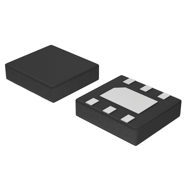
The NTLGF3402PT2G meets the mandatory electrical and mechanical criteria. Although its continuous drain current rating (2.3A) is lower than the FDFM2P110 (3.5A), it maintains identical Vdss, Rds On specification, operating temperature range, and compliance certifications. The NTLGF3402PT2G is classified as Active, ensuring long-term availability and support.
Parameter Comparison
| Parameter | FDFM2P110 | NTLGF3402PT2G | Unit |
|---|---|---|---|
| Manufacturer | onsemi | onsemi | — |
| FET Type | P-Channel | P-Channel | — |
| Drain to Source Voltage (Vdss) | 20 | 20 | V |
| Current - Continuous Drain (Id) @ 25°C | 3.5 | 2.3 | A |
| Rds On (Max) @ Vgs 4.5V | 140 @ 3.5A | 140 @ 2.7A | mOhm |
| Vgs(th) (Max) @ Id | 1.5 @ 250µA | 2.0 @ 250µA | V |
| Gate Charge (Qg) (Max) @ Vgs 4.5V | 4 | 10 | nC |
| Vgs (Max) | ±12 | ±12 | V |
| Input Capacitance (Ciss) @ Vds 10V | 280 | 350 | pF |
| Power Dissipation (Max) | 2 | 1.14 | W |
| Operating Temperature Range | -55 to 150 | -55 to 150 | °C (TJ) |
| Package / Case | 6-WDFN Exposed Pad | 6-VDFN Exposed Pad | 3x3mm |
| Product Status | Obsolete | Active | — |
| RoHS Status | ROHS3 Compliant | ROHS3 Compliant | — |
| Moisture Sensitivity Level (MSL) | 1 (Unlimited) | 1 (Unlimited) | — |
Engineering Selection Recommendations
NTLGF3402PT2G as Primary Substitute:
The NTLGF3402PT2G is the qualified substitute for the obsolete FDFM2P110. Selection is based on the following engineering criteria:
Compliance & Availability:
- Active product status ensures long-term supply chain continuity and manufacturer support
- ROHS3 compliance and MSL Level 1 rating match the original part specifications
- REACH Unaffected status maintains regulatory alignment
Electrical Compatibility:
- Identical Vdss rating (20V) ensures voltage margin preservation in circuit designs
- Rds On specification (140 mOhm) matches the original part at comparable gate-source voltage
- Operating temperature range (-55°C to 150°C TJ) provides thermal equivalence
- Gate-source voltage limits (±12V) are identical
Application Considerations:
- The NTLGF3402PT2G continuous drain current (2.3A) is lower than the FDFM2P110 (3.5A). Circuit designs operating at or below 2.3A continuous current are directly compatible
- Designs requiring the full 3.5A rating of the FDFM2P110 require thermal and current distribution analysis to confirm the NTLGF3402PT2G's 1.14W power dissipation capability
- Gate charge (10 nC vs. 4 nC) is higher, resulting in increased switching losses in high-frequency applications
- Input capacitance (350 pF vs. 280 pF) is higher, affecting gate drive requirements
Package Compatibility:
- Both devices use 3x3mm surface mount packages (6-WDFN and 6-VDFN Exposed Pad variants)
- PCB footprints are compatible; pin assignments require verification against individual datasheets
Frequently Asked Questions (FAQ)
Q: Can the NTLGF3402PT2G directly replace the FDFM2P110 in all applications?
A: Direct replacement is possible for applications where continuous drain current does not exceed 2.3A. Applications requiring the full 3.5A rating of the FDFM2P110 require circuit analysis to confirm thermal and current handling compatibility with the NTLGF3402PT2G's 1.14W power dissipation rating.
Q: What are the key electrical differences between these parts?
A: The primary differences are continuous drain current (3.5A vs. 2.3A), gate charge (4 nC vs. 10 nC), input capacitance (280 pF vs. 350 pF), and power dissipation (2W vs. 1.14W). Vdss, Rds On, operating temperature, and gate-source voltage limits are identical.
Q: Are the packages physically compatible?
A: Both devices use 3x3mm surface mount packages with 6-pin configurations (WDFN and VDFN variants). PCB footprints are compatible. Pin-to-pin functionality must be verified against individual device datasheets to confirm signal routing compatibility.
Q: How does the higher gate charge of the NTLGF3402PT2G affect circuit performance?
A: Higher gate charge (10 nC vs. 4 nC) increases the energy required to switch the device and extends switching time. In high-frequency switching applications, this results in increased gate drive power consumption and potential switching losses. Gate drive circuits must be evaluated for adequate current sourcing capability.
Q: What is the impact of lower power dissipation rating on thermal design?
A: The NTLGF3402PT2G's 1.14W power dissipation rating is lower than the FDFM2P110's 2W rating. Thermal management design must account for this reduced capability. Applications operating near the thermal limits of the original part require thermal analysis to confirm the substitute part's suitability.
Q: Are both parts RoHS compliant?
A: Yes, both the FDFM2P110 and NTLGF3402PT2G are ROHS3 compliant with MSL Level 1 (Unlimited) moisture sensitivity ratings. REACH status is Unaffected for both parts.
Q: Why is the FDFM2P110 obsolete?
A: The FDFM2P110 is classified as obsolete by the manufacturer. The NTLGF3402PT2G represents the active equivalent within onsemi's current product portfolio, ensuring ongoing availability and support for new designs and production continuity.
Alternative Parts

SJ6012L2TP
Littelfuse Inc.
6 Alternative Parts

JMK107BBJ476MA-RE
Taiyo Yuden
10 Alternative Parts

GMK107BBJ475MA-T
Taiyo Yuden
5 Alternative Parts
SJ6020N2ARP
Littelfuse Inc.
3 Alternative Parts
SJ6025R2ATP
Littelfuse Inc.
4 Alternative Parts

2474-05L
API Delevan Inc.
1 Alternative Parts

4590R-684K
API Delevan Inc.
1 Alternative Parts

CM6560R-334
API Delevan Inc.
1 Alternative Parts

CM6460-104
API Delevan Inc.
1 Alternative Parts

5526-12
API Delevan Inc.
1 Alternative Parts