


Request Quote
(Ships tomorrow)
FDD8778 Equivalent & Substitute Parts
Part Overview
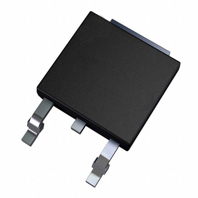
The FDD8778 is an N-Channel MOSFET manufactured by onsemi, rated for 25V drain-to-source voltage with 35A continuous drain current at 25°C. This device is housed in a TO-252AA surface mount package and is part of the PowerTrench® series. The FDD8778 is classified as obsolete, making identification of equivalent substitute components necessary for ongoing design support and procurement continuity. Substitute parts must maintain electrical and mechanical compatibility within the specified parameter ranges to ensure functional equivalence in circuit applications.
Substiute Parts
Key Parameters
| Parameter | Value | Unit |
|---|---|---|
| FET Type | N-Channel | — |
| Drain to Source Voltage (Vdss) | 25 | V |
| Current - Continuous Drain (Id) @ 25°C | 35 | A (Tc) |
| Rds On (Max) @ Id, Vgs | 14 | mOhm @ 35A, 10V |
| Vgs(th) (Max) @ Id | 2.5 | V @ 250µA |
| Gate Charge (Qg) (Max) @ Vgs | 18 | nC @ 10V |
| Power Dissipation (Max) | 39 | W (Tc) |
| Operating Temperature Range | -55 to 175 | °C (TJ) |
| Mounting Type | Surface Mount | — |
| Package / Case | TO-252-3, DPAK (2 Leads + Tab), SC-63 | — |
Substitute Part Grouping Explanation
Substitute parts for the FDD8778 are identified based on strict electrical and mechanical compatibility criteria. The following parameters define the substitution scope:
Electrical Compatibility Criteria:
- FET Type: N-Channel topology required
- Drain to Source Voltage (Vdss): Substitute must equal or exceed 25V
- Continuous Drain Current (Id): Substitute must equal or exceed 35A at 25°C
- Rds On (Max): Substitute must not exceed 14 mOhm @ specified Id and Vgs conditions
- Gate Charge (Qg): Lower or equivalent values acceptable
- Vgs(th): Threshold voltage within ±20V gate voltage range
- Operating Temperature: Must support -55°C to 175°C range
- Power Dissipation: Substitute must support thermal requirements
Mechanical Compatibility Criteria:
- Mounting Type: Surface Mount required
- Package / Case: TO-252-3 DPAK footprint compatibility required
The IPD135N03LGATMA1 meets these criteria as a substitute for the FDD8778.
Parameter Comparison
| Parameter | FDD8778 (onsemi) | IPD135N03LGATMA1 (Infineon) | Unit |
|---|---|---|---|
| Manufacturer Part Number | FDD8778 | IPD135N03LGATMA1 | — |
| Manufacturer | onsemi | Infineon Technologies | — |
| Product Status | Obsolete | Active | — |
| FET Type | N-Channel | N-Channel | — |
| Drain to Source Voltage (Vdss) | 25 | 30 | V |
| Current - Continuous Drain (Id) @ 25°C | 35 | 30 | A (Tc) |
| Rds On (Max) @ Id, Vgs | 14 | 13.5 | mOhm @ rated Id, 10V |
| Vgs(th) (Max) @ Id | 2.5 | 2.2 | V @ 250µA |
| Gate Charge (Qg) (Max) @ Vgs | 18 | 10 | nC @ 10V |
| Vgs (Max) | ±20 | ±20 | V |
| Input Capacitance (Ciss) (Max) @ Vds | 845 | 1000 | pF @ specified Vds |
| Power Dissipation (Max) | 39 | 31 | W (Tc) |
| Operating Temperature Range | -55 to 175 | -55 to 175 | °C (TJ) |
| Mounting Type | Surface Mount | Surface Mount | — |
| Package / Case | TO-252-3, DPAK (2 Leads + Tab), SC-63 | TO-252-3, DPAK (2 Leads + Tab), SC-63 | — |
| RoHS Status | ROHS3 Compliant | ROHS3 Compliant | — |
| REACH Status | REACH Unaffected | REACH Unaffected | — |
Engineering Selection Recommendations
The IPD135N03LGATMA1 from Infineon Technologies is a qualified substitute for the obsolete FDD8778. Selection of this substitute is supported by the following factors:
Product Status Alignment: The IPD135N03LGATMA1 maintains Active product status, ensuring long-term availability and manufacturing support compared to the Obsolete FDD8778.
Electrical Compatibility: The IPD135N03LGATMA1 exceeds the FDD8778 specifications in drain-to-source voltage (30V vs. 25V), providing enhanced voltage margin. While continuous drain current is rated at 30A versus 35A, the on-resistance (Rds On) is superior at 13.5 mOhm compared to 14 mOhm, resulting in lower conduction losses. Gate charge is reduced to 10 nC from 18 nC, improving switching efficiency.
Mechanical Compatibility: Both devices utilize identical TO-252-3 DPAK surface mount packaging, ensuring footprint compatibility without PCB redesign.
Regulatory Compliance: Both parts maintain ROHS3 compliance and REACH Unaffected status, satisfying environmental and regulatory requirements.
Thermal Performance: Operating temperature ranges are identical (-55°C to 175°C), supporting equivalent thermal operating conditions.
Frequently Asked Questions (FAQ)
Q: Can the IPD135N03LGATMA1 directly replace the FDD8778 without circuit modification?
A: The IPD135N03LGATMA1 is mechanically and electrically compatible with the FDD8778 in TO-252-3 DPAK footprint applications. Both devices share identical gate voltage specifications (±20V maximum), threshold voltage characteristics, and operating temperature ranges. No circuit modification is required for direct substitution in standard switching applications.
Q: What is the significance of the higher Vdss rating (30V) on the IPD135N03LGATMA1?
A: The 30V Vdss rating on the IPD135N03LGATMA1 provides additional voltage margin above the FDD8778's 25V specification. This higher rating does not degrade performance in 25V applications and offers enhanced protection against voltage transients and overshoot conditions.
Q: How does the reduced continuous drain current (30A vs. 35A) affect substitution suitability?
A: The IPD135N03LGATMA1 is rated for 30A continuous drain current compared to the FDD8778's 35A. Applications requiring sustained current above 30A at 25°C require thermal analysis to confirm the substitute's adequacy. The superior on-resistance (13.5 mOhm vs. 14 mOhm) partially compensates through reduced conduction losses.
Q: What advantage does the lower gate charge (10 nC vs. 18 nC) provide?
A: Reduced gate charge on the IPD135N03LGATMA1 decreases switching losses and reduces gate driver power requirements. This results in improved overall circuit efficiency and reduced thermal stress on gate drive circuitry.
Q: Are there any compliance or certification differences between these parts?
A: Both the FDD8778 and IPD135N03LGATMA1 maintain ROHS3 compliance and REACH Unaffected status. No compliance differences exist between these devices.
Q: What is the impact of higher input capacitance (1000 pF vs. 845 pF) on the IPD135N03LGATMA1?
A: The slightly elevated input capacitance on the IPD135N03LGATMA1 requires marginally higher gate charge energy during switching transitions. This difference is offset by the absolute gate charge reduction (10 nC vs. 18 nC), resulting in net improvement in switching performance.
Q: Is the IPD135N03LGATMA1 available in the same packaging format?
A: Yes. Both devices are supplied in TO-252-3 DPAK surface mount packaging with identical lead configuration (2 Leads + Tab, SC-63). PCB footprints are directly compatible without modification.
Alternative Parts

SJ6012L2TP
Littelfuse Inc.
6 Alternative Parts

JMK107BBJ476MA-RE
Taiyo Yuden
10 Alternative Parts

GMK107BBJ475MA-T
Taiyo Yuden
5 Alternative Parts
SJ6020N2ARP
Littelfuse Inc.
3 Alternative Parts
SJ6025R2ATP
Littelfuse Inc.
4 Alternative Parts

2474-05L
API Delevan Inc.
1 Alternative Parts

4590R-684K
API Delevan Inc.
1 Alternative Parts

CM6560R-334
API Delevan Inc.
1 Alternative Parts

CM6460-104
API Delevan Inc.
1 Alternative Parts

5526-12
API Delevan Inc.
1 Alternative Parts