


Request Quote
(Ships tomorrow)
FDD86110 Equivalent & Substitute Parts
Part Overview
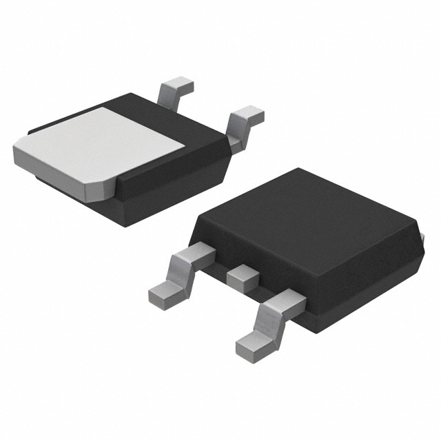
The FDD86110 is an N-Channel MOSFET manufactured by onsemi, rated for 100V drain-to-source voltage with continuous drain current of 12.5A at Ta and 50A at Tc. This device operates in the PowerTrench® series and is housed in a Surface Mount TO-252AA (DPAK) package. The part is Active in product status and RoHS3 compliant. Substitute parts are identified when equivalent electrical performance and mechanical compatibility are required due to inventory constraints, design optimization, or application-specific requirements within the specified parameter ranges.
Substiute Parts
Key Parameters
| Parameter | Value | Unit |
|---|---|---|
| Drain to Source Voltage (Vdss) | 100 | V |
| Continuous Drain Current @ 25°C (Ta) | 12.5 | A |
| Continuous Drain Current @ 25°C (Tc) | 50 | A |
| Rds On (Max) @ Id, Vgs | 10.2 mOhm @ 12.5A, 10V | mOhm |
| Gate Threshold Voltage (Vgs(th)) @ Id | 4 | V @ 250µA |
| Gate Charge (Qg) @ Vgs | 35 | nC @ 10V |
| Input Capacitance (Ciss) @ Vds | 2265 | pF @ 50V |
| Power Dissipation (Max) @ Ta | 3.1 | W |
| Power Dissipation (Max) @ Tc | 127 | W |
| Operating Temperature Range | -55 to 150 | °C (TJ) |
| Package Type | TO-252-3, DPAK (2 Leads + Tab) | Surface Mount |
| RoHS Status | ROHS3 Compliant | - |
| Moisture Sensitivity Level | 1 (Unlimited) | - |
Substitute Part Grouping Explanation
Substitute parts for the FDD86110 are qualified based on the following criteria:
Electrical Compatibility Parameters:
- Drain to Source Voltage (Vdss): Must equal or exceed 100V
- FET Type: N-Channel MOSFET technology
- Gate Voltage Range (Vgs Max): ±20V compatibility
- Operating Temperature Range: Must support minimum -55°C to 150°C
- Package Type: TO-252-3 DPAK (2 Leads + Tab) form factor
- Mounting Type: Surface Mount
Regulatory & Compliance Parameters:
- RoHS3 Compliance: Required
- Moisture Sensitivity Level: MSL 1 (Unlimited)
- ECCN Classification: EAR99
- Product Status: Active
Performance Consideration Parameters:
- Rds On (Max): Substitutes must maintain acceptable on-resistance characteristics
- Gate Charge (Qg): Switching performance indicator
- Input Capacitance (Ciss): Load capacitance consideration
- Power Dissipation: Thermal management capability
Substitutes are grouped by their ability to meet or exceed these parameters while maintaining functional equivalence in typical application circuits.
Parameter Comparison
| Parameter | FDD86110 (onsemi) | STD100N10F7 (STMicroelectronics) | TK33S10N1Z,LQ (Toshiba) |
|---|---|---|---|
| Manufacturer | onsemi | STMicroelectronics | Toshiba Semiconductor and Storage |
| Drain to Source Voltage (Vdss) | 100 V | 100 V | 100 V |
| Continuous Drain Current @ 25°C (Ta) | 12.5 A | - | 33 A |
| Continuous Drain Current @ 25°C (Tc) | 50 A | 80 A | - |
| Rds On (Max) @ Id, Vgs | 10.2 mOhm @ 12.5A, 10V | 8 mOhm @ 40A, 10V | 9.7 mOhm @ 16.5A, 10V |
| Gate Threshold Voltage (Vgs(th)) @ Id | 4 V @ 250µA | 4.5 V @ 250µA | 4 V @ 500µA |
| Gate Charge (Qg) @ Vgs | 35 nC @ 10V | 61 nC @ 10V | 28 nC @ 10V |
| Input Capacitance (Ciss) @ Vds | 2265 pF @ 50V | 4369 pF @ 50V | 2050 pF @ 10V |
| Power Dissipation (Max) @ Tc | 127 W | 120 W | 125 W |
| Operating Temperature Range | -55 to 150°C (TJ) | -55 to 175°C (TJ) | -55 to 175°C (TJ) |
| Package Type | TO-252-3, DPAK (2 Leads + Tab) | TO-252-3, DPAK (2 Leads + Tab) | TO-252-3, DPAK (2 Leads + Tab) |
| Mounting Type | Surface Mount | Surface Mount | Surface Mount |
| RoHS Status | ROHS3 Compliant | ROHS3 Compliant | ROHS3 Compliant |
| Moisture Sensitivity Level | 1 (Unlimited) | 1 (Unlimited) | 1 (Unlimited) |
| Product Status | Active | Active | Active |
Engineering Selection Recommendations
STD100N10F7 (STMicroelectronics): This substitute is qualified for applications requiring higher continuous drain current capacity at Tc (80A versus 50A). The STD100N10F7 operates within the same 100V Vdss rating and maintains compatible gate voltage specifications. The device is RoHS3 compliant with MSL 1 rating and Active product status. Operating temperature range extends to 175°C, providing additional thermal margin. The lower Rds On value (8 mOhm) indicates improved efficiency characteristics. Gate charge is elevated (61 nC), which may impact switching frequency performance in high-speed applications.
TK33S10N1Z,LQ (Toshiba Semiconductor and Storage): This substitute is qualified for applications where gate charge minimization is prioritized (28 nC versus 35 nC). The TK33S10N1Z,LQ maintains 100V Vdss rating and compatible gate voltage specifications. The device is RoHS3 compliant with MSL 1 rating and Active product status. Continuous drain current at Ta is 33A, providing intermediate current capacity. Input capacitance is lower (2050 pF), supporting faster switching transitions. Operating temperature range extends to 175°C. Rds On is comparable (9.7 mOhm), maintaining efficiency characteristics similar to the primary part.
Both substitutes maintain electrical and mechanical compatibility with the FDD86110 within the specified parameter ranges and regulatory requirements.
Frequently Asked Questions (FAQ)
Q: Can the STD100N10F7 be used as a direct replacement for the FDD86110?
A: The STD100N10F7 is electrically compatible as a substitute. Both devices share identical 100V Vdss rating, compatible gate voltage specifications (±20V), and identical DPAK package form factor. The STD100N10F7 provides higher continuous drain current capacity (80A at Tc versus 50A at Tc) and lower on-resistance (8 mOhm versus 10.2 mOhm). Both are RoHS3 compliant with MSL 1 rating and Active product status. Circuit board layout and thermal management design remain compatible.
Q: What are the key differences between the TK33S10N1Z,LQ and FDD86110?
A: The TK33S10N1Z,LQ differs in gate charge (28 nC versus 35 nC) and input capacitance (2050 pF versus 2265 pF), resulting in faster switching characteristics. Continuous drain current at Ta is 33A compared to 12.5A. On-resistance is comparable (9.7 mOhm versus 10.2 mOhm). Both devices maintain 100V Vdss rating, ±20V gate voltage range, and identical DPAK package specifications. Regulatory compliance and MSL ratings are equivalent.
Q: Are all three devices compatible with the same PCB footprint?
A: Yes. The FDD86110, STD100N10F7, and TK33S10N1Z,LQ all use the TO-252-3 DPAK (2 Leads + Tab) package form factor. Surface mount footprints are mechanically identical, allowing direct substitution without PCB redesign.
Q: What is the operating temperature range compatibility?
A: The FDD86110 operates from -55°C to 150°C (TJ). The STD100N10F7 and TK33S10N1Z,LQ both extend to 175°C (TJ). All three devices support the FDD86110 operating range. Applications requiring operation above 150°C benefit from the extended range of the substitute parts.
Q: How do gate charge specifications affect circuit performance?
A: Gate charge (Qg) determines the energy required to switch the MOSFET on and off. The FDD86110 requires 35 nC at 10V. The TK33S10N1Z,LQ requires 28 nC, enabling faster switching with lower gate drive power. The STD100N10F7 requires 61 nC, resulting in slower switching transitions. Gate driver circuits must supply sufficient current to meet these charge requirements within the desired switching frequency.
Q: Are moisture sensitivity levels equivalent across all three devices?
A: Yes. The FDD86110, STD100N10F7, and TK33S10N1Z,LQ all carry MSL 1 (Unlimited) rating, indicating no moisture sensitivity restrictions. Standard handling and storage procedures apply uniformly across all three devices.
Q: What regulatory certifications apply to these substitutes?
A: All three devices are RoHS3 compliant and carry ECCN EAR99 classification. REACH status is unaffected for all parts. HTSUS code 8541.29.0095 applies uniformly. All devices maintain Active product status with established supply chains.
Alternative Parts

SJ6012L2TP
Littelfuse Inc.
6 Alternative Parts

JMK107BBJ476MA-RE
Taiyo Yuden
10 Alternative Parts

GMK107BBJ475MA-T
Taiyo Yuden
5 Alternative Parts
SJ6020N2ARP
Littelfuse Inc.
3 Alternative Parts
SJ6025R2ATP
Littelfuse Inc.
4 Alternative Parts

2474-05L
API Delevan Inc.
1 Alternative Parts

4590R-684K
API Delevan Inc.
1 Alternative Parts

CM6560R-334
API Delevan Inc.
1 Alternative Parts

CM6460-104
API Delevan Inc.
1 Alternative Parts

5526-12
API Delevan Inc.
1 Alternative Parts