


Request Quote
(Ships tomorrow)
FDD8451 Equivalent & Substitute Parts
Part Overview
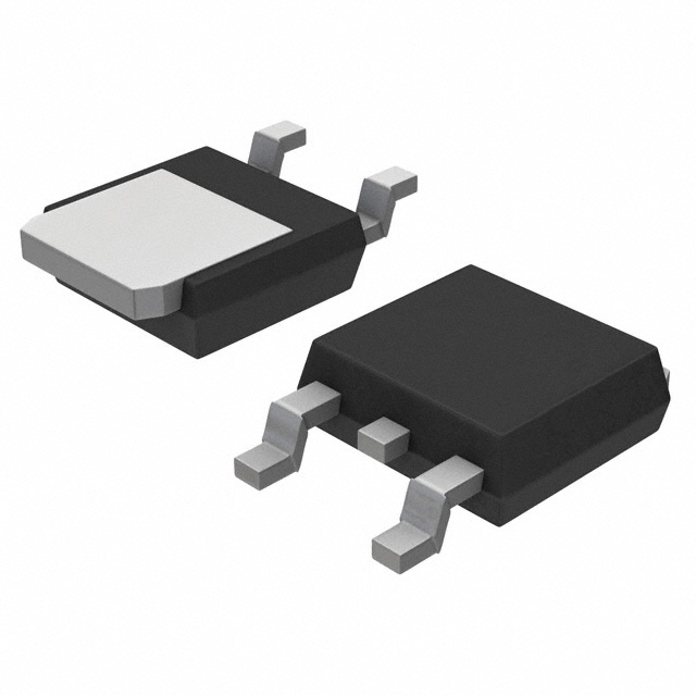
The FDD8451 is an N-Channel MOSFET manufactured by onsemi, rated for 40V drain-to-source voltage with continuous drain current of 9A at Ta and 28A at Tc. This device is packaged in TO-252AA (DPAK) surface mount configuration and is classified as obsolete. The FDD8451 belongs to the PowerTrench® series and is ROHS3 compliant with unlimited moisture sensitivity level.
Due to the obsolete product status of the FDD8451, equivalent and substitute parts are necessary to maintain design continuity and ensure component availability for new production runs and field replacements.
Substiute Parts
Key Parameters
| Parameter | FDD8451 Value | Unit |
|---|---|---|
| Drain to Source Voltage (Vdss) | 40 | V |
| Continuous Drain Current @ 25°C | 9A (Ta), 28A (Tc) | A |
| Rds On (Max) @ Id, Vgs | 24 mOhm @ 9A, 10V | mOhm |
| Gate Charge (Qg) @ Vgs | 20 nC @ 10V | nC |
| Input Capacitance (Ciss) @ Vds | 990 pF @ 20V | pF |
| Power Dissipation (Max) | 30 | W (Tc) |
| Operating Temperature Range | -55 to 150 | °C (TJ) |
| Package Type | TO-252-3 (DPAK) | — |
| Vgs(th) @ Id | 3 @ 250µA | V |
| Vgs (Max) | ±20 | V |
Substitute Part Grouping Explanation
Substitution of the FDD8451 is determined by the following critical electrical and mechanical parameters:
Primary Substitution Criteria:
- Drain to Source Voltage (Vdss): Must equal or exceed 40V
- Package Type: Must be TO-252-3 (DPAK) surface mount configuration
- FET Type: N-Channel MOSFET technology
- Gate Threshold Voltage (Vgs(th)): Must be compatible within ±20V maximum gate voltage specification
- Operating Temperature Range: Must support -55°C to 150°C (TJ)
- RoHS3 Compliance: Required for regulatory compatibility
Secondary Compatibility Parameters:
- Continuous Drain Current (Id): Substitute must meet or exceed application requirements
- Rds On (Max): Lower or equal values indicate improved performance
- Gate Charge (Qg): Lower values reduce switching losses
- Input Capacitance (Ciss): Affects gate drive requirements
The substitute parts listed below satisfy the primary substitution criteria and maintain electrical compatibility within the specified parameter ranges.
Parameter Comparison
| Parameter | FDD8451 (onsemi) | DMN4026SK3-13 (Diodes) | DMN4040SK3-13 (Diodes) | PJD25N04_L2_00001 (Panjit) | RSD200N05TL (Rohm) |
|---|---|---|---|---|---|
| Manufacturer | onsemi | Diodes Incorporated | Diodes Incorporated | Panjit International Inc. | Rohm Semiconductor |
| Vdss (V) | 40 | 40 | 40 | 40 | 45 |
| Id @ 25°C (A) | 9 (Ta), 28 (Tc) | 28 (Tc) | 6 (Ta) | 5.9 (Ta), 21 (Tc) | 20 (Ta) |
| Rds On (Max) @ Id, Vgs (mOhm) | 24 @ 9A, 10V | 24 @ 6A, 10V | 30 @ 12A, 10V | 32 @ 12A, 10V | 28 @ 20A, 10V |
| Qg (Max) @ Vgs (nC) | 20 @ 10V | 21.3 @ 10V | 18.6 @ 10V | 4.4 @ 4.5V | 12 @ 5V |
| Ciss (Max) @ Vds (pF) | 990 @ 20V | 1181 @ 20V | 945 @ 20V | 425 @ 25V | 950 @ 10V |
| Power Dissipation (Max) (W) | 30 (Tc) | 1.6 (Ta) | 1.71 (Ta) | 2 (Ta), 25 (Tc) | 20 (Tc) |
| Operating Temperature (°C) | -55 to 150 | -55 to 150 | -55 to 150 | -55 to 150 | -55 to 150 |
| Package | TO-252-3 (DPAK) | TO-252-3 (DPAK) | TO-252-3 (DPAK) | TO-252-3 (DPAK) | TO-252-3 (DPAK) |
| Vgs(th) @ Id (V) | 3 @ 250µA | 3 @ 250µA | 3 @ 250µA | 2.5 @ 250µA | 2.5 @ 1mA |
| Vgs (Max) (V) | ±20 | ±20 | ±20 | ±20 | ±20 |
| Product Status | Obsolete | Active | Active | Active | Active |
| RoHS3 Compliance | Yes | Yes | Yes | Yes | Yes |
| MSL Rating | 1 (Unlimited) | 1 (Unlimited) | 1 (Unlimited) | 1 (Unlimited) | 1 (Unlimited) |
Engineering Selection Recommendations
DMN4026SK3-13 (Diodes Incorporated)
The DMN4026SK3-13 provides the closest electrical match to the FDD8451 with identical Vdss (40V) and Rds On specifications (24 mOhm @ 10V). This device is active in production status and maintains full RoHS3 compliance. The DMN4026SK3-13 supports continuous drain current of 28A at Tc, matching the FDD8451 thermal performance specification. Gate charge and input capacitance values are within 7% of the original device. This substitute is suitable for direct replacement in applications where the 28A (Tc) rating is the primary design parameter.
DMN4040SK3-13 (Diodes Incorporated)
The DMN4040SK3-13 maintains identical Vdss (40V) and package configuration with active product status. This device is appropriate for applications with lower continuous drain current requirements (6A at Ta). The Rds On specification is 30 mOhm at 10V, representing a 25% increase in on-resistance compared to the FDD8451. Gate charge is 18.6 nC, approximately 7% lower than the original device. This substitute is suitable for lower-power applications where the reduced current rating is acceptable.
PJD25N04_L2_00001 (Panjit International Inc.)
The PJD25N04_L2_00001 meets the 40V Vdss requirement and maintains TO-252-3 package compatibility. This device is active in production and RoHS3 compliant. The continuous drain current specification is 5.9A at Ta and 21A at Tc, providing performance comparable to the FDD8451 thermal rating. The Rds On specification is 32 mOhm at 10V. Gate charge is significantly lower at 4.4 nC at 4.5V, and input capacitance is reduced to 425 pF. This substitute is suitable for applications where lower gate charge and capacitance are beneficial for gate drive circuit optimization.
RSD200N05TL (Rohm Semiconductor)
The RSD200N05TL exceeds the Vdss requirement at 45V and is active in production with full RoHS3 compliance. This device supports 20A continuous drain current at Ta and 20W power dissipation at Tc. The Rds On specification is 28 mOhm at 10V. Gate charge is 12 nC at 5V, and input capacitance is 950 pF at 10V. The package is specified as CPT3 surface mount, which is mechanically compatible with TO-252-3 (DPAK) footprints. This substitute is suitable for applications requiring higher voltage margin and improved thermal performance.
Frequently Asked Questions (FAQ)
Q: Can the DMN4026SK3-13 be used as a direct replacement for the FDD8451?
A: Yes. The DMN4026SK3-13 matches the FDD8451 in Vdss (40V), Rds On (24 mOhm @ 10V), package type (TO-252-3), and operating temperature range (-55°C to 150°C). Both devices are RoHS3 compliant with MSL 1 rating. The electrical parameters are within acceptable tolerance for direct substitution.
Q: What is the primary difference between the DMN4026SK3-13 and DMN4040SK3-13?
A: The primary difference is continuous drain current rating. The DMN4026SK3-13 is rated for 28A at Tc, while the DMN4040SK3-13 is rated for 6A at Ta. The DMN4040SK3-13 also has higher Rds On (30 mOhm vs. 24 mOhm). Selection depends on the application's current requirements.
Q: Is the RSD200N05TL package compatible with FDD8451 PCB layouts?
A: The RSD200N05TL uses CPT3 package, which is mechanically compatible with TO-252-3 (DPAK) footprints. Pin configuration and lead spacing are equivalent, allowing PCB layout compatibility without modification.
Q: Why does the PJD25N04_L2_00001 have lower gate charge than the FDD8451?
A: Gate charge is a device-specific parameter determined by the internal gate structure and capacitance characteristics. The PJD25N04_L2_00001 is specified at 4.4 nC at 4.5V, compared to the FDD8451 at 20 nC at 10V. Lower gate charge reduces switching losses and gate drive power requirements.
Q: Are all substitute parts RoHS3 compliant?
A: Yes. All substitute parts listed (DMN4026SK3-13, DMN4040SK3-13, PJD25N04_L2_00001, and RSD200N05TL) are RoHS3 compliant with MSL 1 (Unlimited) moisture sensitivity level, matching the FDD8451 compliance status.
Q: What is the significance of Vdss rating differences between substitutes?
A: Vdss (Drain to Source Voltage) is the maximum voltage the device can withstand between drain and source terminals. The FDD8451 is rated for 40V. The RSD200N05TL is rated for 45V, providing 5V additional voltage margin. All substitutes meet or exceed the 40V requirement, ensuring compatibility with 40V circuit designs.
Q: Can the DMN4040SK3-13 replace the FDD8451 in high-current applications?
A: No. The DMN4040SK3-13 is rated for 6A continuous drain current at Ta, significantly lower than the FDD8451's 9A (Ta) and 28A (Tc) ratings. This substitute is suitable only for applications with lower current requirements.
Q: How do input capacitance differences affect circuit performance?
A: Input capacitance (Ciss) affects gate drive circuit design and switching speed. The FDD8451 has 990 pF at 20V. Substitutes range from 425 pF (PJD25N04_L2_00001) to 1181 pF (DMN4026SK3-13). Lower capacitance reduces gate drive power and improves switching speed; higher capacitance requires stronger gate drive circuits.
Q: What is the impact of Rds On variation among substitutes?
A: Rds On (on-resistance) directly affects power dissipation and heat generation. Lower Rds On values reduce conduction losses. The FDD8451 and DMN4026SK3-13 both specify 24 mOhm, while the DMN4040SK3-13 specifies 30 mOhm and the PJD25N04_L2_00001 specifies 32 mOhm. Higher Rds On values increase power dissipation in high-current applications.
Q: Are all substitutes available in the same packaging format?
A: All substitutes use TO-252-3 (DPAK) surface mount packaging, which is mechanically and electrically compatible with the FDD8451. The RSD200N05TL is specified as CPT3, which is equivalent to TO-252-3 in form factor and pin configuration.
Alternative Parts

SJ6012L2TP
Littelfuse Inc.
6 Alternative Parts

JMK107BBJ476MA-RE
Taiyo Yuden
10 Alternative Parts

GMK107BBJ475MA-T
Taiyo Yuden
5 Alternative Parts
SJ6020N2ARP
Littelfuse Inc.
3 Alternative Parts
SJ6025R2ATP
Littelfuse Inc.
4 Alternative Parts

2474-05L
API Delevan Inc.
1 Alternative Parts

4590R-684K
API Delevan Inc.
1 Alternative Parts

CM6560R-334
API Delevan Inc.
1 Alternative Parts

CM6460-104
API Delevan Inc.
1 Alternative Parts

5526-12
API Delevan Inc.
1 Alternative Parts