


Request Quote
(Ships tomorrow)
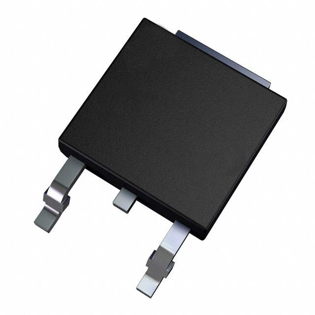
FDD5670 N-Channel MOSFET 60V 52A Equivalent & Substitute Parts
Part Overview
The FDD5670 is an N-Channel MOSFET manufactured by onsemi in the PowerTrench® series, rated for 60V drain-to-source voltage with 52A continuous drain current at 25°C. The device is housed in a TO-252AA surface mount package (DPAK configuration) and is designed for high-current switching applications.
The FDD5670 carries an Obsolete product status. Identification of equivalent and substitute parts is necessary to ensure design continuity, maintain supply chain reliability, and support ongoing production requirements for applications utilizing this component.
Substiute Parts
Key Parameters
| Parameter | FDD5670 Value | Unit |
|---|---|---|
| Drain-to-Source Voltage (Vdss) | 60 | V |
| Continuous Drain Current @ 25°C (Id) | 52 (Ta) | A |
| On-State Resistance @ 10A, 10V (Rds On Max) | 15 | mOhm |
| Gate Threshold Voltage @ 250µA (Vgs(th) Max) | 4 | V |
| Gate Charge @ 10V (Qg Max) | 73 | nC |
| Input Capacitance @ 15V (Ciss Max) | 2739 | pF |
| Power Dissipation (Tc) | 83 | W |
| Operating Temperature Range | -55 to 175 | °C |
| Package Type | TO-252-3 DPAK | — |
| Mounting Type | Surface Mount | — |
| RoHS Status | ROHS3 Compliant | — |
Substitute Part Grouping Explanation
Substitution of the FDD5670 is determined by the following critical electrical and mechanical parameters:
Voltage Rating Compatibility: All substitute parts must maintain a Vdss rating of 60V or higher to ensure safe operation within the original design envelope.
Current Handling Capacity: Substitute parts must support continuous drain current ratings at or above 52A (measured at Ta or Tc conditions) to maintain equivalent current-carrying capability.
On-State Resistance (Rds On): The maximum on-state resistance must not exceed the original specification to prevent excessive power dissipation and thermal stress in the application circuit.
Package and Mounting: All substitutes must use the TO-252-3 DPAK surface mount package to ensure mechanical and thermal compatibility with existing PCB layouts and thermal management solutions.
Gate Drive Characteristics: Gate threshold voltage and gate charge specifications must remain within compatible ranges to ensure proper switching behavior with existing gate drive circuitry.
Temperature Range: Operating temperature range must encompass the original -55°C to 175°C specification to maintain reliability across the full application temperature envelope.
Compliance Standards: All substitute parts must maintain RoHS3 compliance and REACH unaffected status to satisfy regulatory and supply chain requirements.
Parameter Comparison
| Parameter | FDD5670 | FDD13AN06A0 | BUK7212-55B,118 | IPD50N06S4L12ATMA2 | STD35NF06LT4 | STD60NF06T4 | STD70N6F3 | Unit |
|---|---|---|---|---|---|---|---|---|
| Manufacturer | onsemi | onsemi | Nexperia USA Inc. | Infineon Technologies | STMicroelectronics | STMicroelectronics | STMicroelectronics | — |
| Vdss | 60 | 60 | 55 | 60 | 60 | 60 | 60 | V |
| Id (Continuous Drain Current) | 52 (Ta) | 50 (Tc) | 75 (Tc) | 50 (Tc) | 35 (Tc) | 60 (Tc) | 70 (Tc) | A |
| Rds On (Max) | 15 @ 10A, 10V | 13.5 @ 50A, 10V | 12 @ 25A, 10V | 12 @ 50A, 10V | 17 @ 17.5A, 10V | 16 @ 30A, 10V | 10.5 @ 35A, 10V | mOhm |
| Vgs(th) (Max) | 4 @ 250µA | 4 @ 250µA | 4 @ 1mA | 2.2 @ 20µA | 2.5 @ 250µA | 4 @ 250µA | 4 @ 250µA | V |
| Qg (Max) | 73 @ 10V | 29 @ 10V | 35 @ 10V | 40 @ 10V | 33 @ 4.5V | 66 @ 10V | 35 @ 10V | nC |
| Ciss (Max) | 2739 @ 15V | 1350 @ 25V | 2453 @ 25V | 2890 @ 25V | 1700 @ 25V | 1810 @ 25V | 2200 @ 25V | pF |
| Power Dissipation (Tc) | 83 | 115 | 167 | 50 | 80 | 110 | 110 | W |
| Operating Temperature Range | -55 to 175 | -55 to 175 | -55 to 185 | -55 to 175 | -55 to 175 | -55 to 175 | -55 to 175 | °C |
| Package | TO-252-3 DPAK | TO-252-3 DPAK | TO-252-3 DPAK | TO-252-3 DPAK | TO-252-3 DPAK | TO-252-3 DPAK | TO-252-3 DPAK | — |
| Product Status | Obsolete | Active | Obsolete | Active | Active | Active | Obsolete | — |
| RoHS Status | ROHS3 Compliant | ROHS3 Compliant | ROHS3 Compliant | ROHS3 Compliant | ROHS3 Compliant | ROHS3 Compliant | ROHS3 Compliant | — |
Engineering Selection Recommendations
Primary Substitute: STD60NF06T4 (STMicroelectronics)
The STD60NF06T4 is the recommended primary substitute for the FDD5670. This device maintains identical voltage rating (60V Vdss), exceeds the continuous drain current requirement (60A Tc versus 52A Ta), and operates within the same temperature range (-55°C to 175°C). The STD60NF06T4 carries Active product status, ensuring long-term availability and supply chain stability. RoHS3 compliance and REACH unaffected status align with regulatory requirements. The on-state resistance of 16 mOhm at 30A, 10V is comparable to the original specification, and the gate charge of 66 nC at 10V closely matches the FDD5670 at 73 nC.
Secondary Substitute: FDD13AN06A0 (onsemi)
The FDD13AN06A0 is an onsemi alternative within the same PowerTrench® series, offering Active product status. This device maintains 60V Vdss rating and supports 50A continuous drain current at Tc, meeting the original 52A Ta specification. The on-state resistance of 13.5 mOhm at 50A, 10V is superior to the original, and gate charge is significantly reduced to 29 nC at 10V, enabling faster switching. Operating temperature range matches the original specification. RoHS3 compliance and REACH unaffected status are maintained.
Tertiary Substitute: STD70N6F3 (STMicroelectronics)
The STD70N6F3 provides higher current capability (70A Tc) and superior on-state resistance (10.5 mOhm at 35A, 10V) compared to the FDD5670. Voltage rating remains at 60V Vdss, and operating temperature range is identical. However, this device carries Obsolete product status, limiting its suitability for new designs requiring long-term supply assurance. RoHS3 compliance and REACH unaffected status are maintained.
Alternative Substitute: IPD50N06S4L12ATMA2 (Infineon Technologies)
The IPD50N06S4L12ATMA2 from Infineon's OptiMOS™ series maintains 60V Vdss and supports 50A continuous drain current at Tc. This device carries Active product status and includes AEC-Q101 automotive qualification. On-state resistance of 12 mOhm at 50A, 10V is superior to the original. Gate threshold voltage is lower at 2.2V, which may require gate drive circuit evaluation. Operating temperature range matches the original specification. RoHS3 compliance and REACH unaffected status are maintained.
Alternative Substitute: STD35NF06LT4 (STMicroelectronics)
The STD35NF06LT4 maintains 60V Vdss and operates within the same temperature range. However, continuous drain current is limited to 35A at Tc, which is below the original 52A specification. This device is suitable only for applications where current requirements can be reduced or where thermal management allows operation at lower current levels. Active product status and RoHS3 compliance are maintained.
Not Recommended: BUK7212-55B,118 (Nexperia USA Inc.)
The BUK7212-55B,118 has a reduced Vdss rating of 55V, which is below the original 60V specification. While current capability (75A Tc) and on-state resistance (12 mOhm) are superior, the lower voltage rating creates design risk. Obsolete product status further limits suitability. This device is not recommended as a primary substitute.
Frequently Asked Questions (FAQ)
Q: Can the FDD5670 be directly replaced with the STD60NF06T4?
A: Yes. Both devices maintain identical 60V Vdss rating, TO-252-3 DPAK package configuration, and -55°C to 175°C operating temperature range. The STD60NF06T4 meets or exceeds all critical electrical parameters including continuous drain current (60A Tc versus 52A Ta) and on-state resistance specifications. RoHS3 compliance is maintained. Direct substitution is supported without circuit modification.
Q: What is the primary advantage of using FDD13AN06A0 over the original FDD5670?
A: The FDD13AN06A0 offers Active product status, ensuring long-term availability compared to the Obsolete FDD5670. Additionally, gate charge is reduced from 73 nC to 29 nC, enabling faster switching transitions and potentially reducing switching losses. On-state resistance is improved to 13.5 mOhm at 50A, 10V. Both devices are from onsemi's PowerTrench® series and maintain identical voltage and temperature specifications.
Q: Why is the BUK7212-55B,118 not recommended as a substitute?
A: The BUK7212-55B,118 has a Vdss rating of 55V, which is 5V below the original FDD5670 specification of 60V. This reduced voltage margin creates design risk in applications where transient overvoltage conditions may occur. Additionally, the device carries Obsolete product status, limiting supply chain reliability. Substitution would require circuit redesign to accommodate the lower voltage rating.
Q: Are all substitute parts available in the same package configuration?
A: Yes. All substitute parts listed are housed in the TO-252-3 DPAK surface mount package, ensuring mechanical and thermal compatibility with existing PCB layouts. Pin configuration and thermal pad dimensions remain consistent across all alternatives, supporting direct board-level substitution without layout modification.
Q: What is the impact of different gate charge specifications on circuit design?
A: Gate charge (Qg) determines the amount of charge required to switch the MOSFET from off to on state. The FDD5670 requires 73 nC at 10V, while alternatives such as FDD13AN06A0 require only 29 nC. Lower gate charge enables faster switching with reduced gate drive current requirements. However, existing gate drive circuits designed for the FDD5670 will function with lower gate charge devices without modification, though switching speed may increase. Gate drive circuit evaluation is recommended when transitioning to devices with significantly different gate charge specifications.
Q: Can the IPD50N06S4L12ATMA2 be used in automotive applications?
A: Yes. The IPD50N06S4L12ATMA2 carries AEC-Q101 automotive qualification, making it suitable for automotive applications. However, the original FDD5670 does not carry automotive qualification. If the application is non-automotive, automotive-qualified alternatives provide additional reliability assurance. If the application is automotive and the FDD5670 was previously used, verification of design compliance with automotive standards is recommended before substitution.
Q: What is the significance of product status (Active versus Obsolete) in component selection?
A: Product status indicates manufacturer support and supply chain availability. Active status devices are in current production with long-term availability assurance. Obsolete devices are no longer manufactured and available only from existing inventory. For new designs or long-term production requirements, Active status devices (STD60NF06T4, FDD13AN06A0, IPD50N06S4L12ATMA2, STD35NF06LT4) are preferred. Obsolete devices (FDD5670, BUK7212-55B,118, STD70N6F3) are suitable only for existing inventory management or short-term production runs.
Q: How do on-state resistance differences affect thermal performance?
A: On-state resistance (Rds On) directly determines power dissipation during conduction: P = I²R. Lower Rds On reduces heat generation. The FDD5670 specifies 15 mOhm at 10A, 10V. Alternatives such as STD70N6F3 (10.5 mOhm) and IPD50N06S4L12ATMA2 (12 mOhm) generate less heat at equivalent current levels, improving thermal performance. Conversely, STD35NF06LT4 (17 mOhm) generates slightly more heat. In thermally constrained applications, lower Rds On devices reduce cooling requirements and improve reliability.
Q: Is RoHS3 compliance maintained across all substitute parts?
A: Yes. All substitute parts listed maintain RoHS3 compliance and REACH unaffected status, matching the original FDD5670 specification. This ensures regulatory compliance for applications subject to RoHS and REACH requirements without additional material or process changes.
Alternative Parts

SJ6012L2TP
Littelfuse Inc.
6 Alternative Parts

JMK107BBJ476MA-RE
Taiyo Yuden
10 Alternative Parts

GMK107BBJ475MA-T
Taiyo Yuden
5 Alternative Parts
SJ6020N2ARP
Littelfuse Inc.
3 Alternative Parts
SJ6025R2ATP
Littelfuse Inc.
4 Alternative Parts

2474-05L
API Delevan Inc.
1 Alternative Parts

4590R-684K
API Delevan Inc.
1 Alternative Parts

CM6560R-334
API Delevan Inc.
1 Alternative Parts

CM6460-104
API Delevan Inc.
1 Alternative Parts

5526-12
API Delevan Inc.
1 Alternative Parts