


Request Quote
(Ships tomorrow)
FDC6320C Equivalent & Substitute Parts
Part Overview
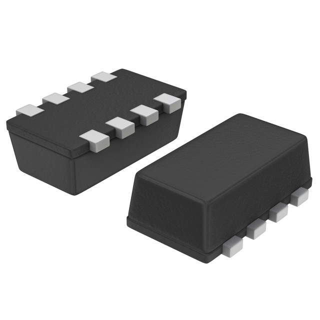
The FDC6320C is an N and P-Channel MOSFET array manufactured by onsemi, housed in a SuperSOT™-6 surface mount package. This device integrates complementary channel MOSFETs with a maximum drain-source voltage rating of 25V and continuous drain current capabilities of 220mA (N-channel) and 120mA (P-channel). The FDC6320C is classified as obsolete, making identification of functionally equivalent alternatives necessary for ongoing design support and production continuity.
Substiute Parts
Key Parameters
| Parameter | Value | Unit |
|---|---|---|
| Drain to Source Voltage (Vdss) | 25 | V |
| Continuous Drain Current (Id) @ 25°C | 220mA (N-ch), 120mA (P-ch) | A |
| On-Resistance (Rds On) @ Id, Vgs | 4Ω @ 400mA, 4.5V | Ω |
| Gate Threshold Voltage (Vgs(th)) @ Id | 1.5V @ 250µA | V |
| Gate Charge (Qg) @ Vgs | 0.4nC @ 4.5V | nC |
| Input Capacitance (Ciss) @ Vds | 9.5pF @ 10V | pF |
| Maximum Power Dissipation | 700 | mW |
| Operating Temperature Range | -55 to 150 | °C |
| Package Type | SOT-23-6 Thin (SuperSOT™-6) | — |
| Configuration | N and P-Channel | — |
| FET Feature | Logic Level Gate | — |
Substitute Part Grouping Explanation
Substitution of the FDC6320C is determined by electrical and mechanical compatibility across the following critical parameters:
Electrical Compatibility Criteria:
- Drain-Source Voltage (Vdss) rating must equal or exceed 25V
- Continuous drain current must meet or exceed the application requirement (220mA N-channel, 120mA P-channel)
- Gate threshold voltage (Vgs(th)) must be compatible with logic-level gate drive circuits
- On-resistance characteristics must support the intended switching and power dissipation profile
- Configuration must maintain N and P-Channel complementary topology
Mechanical Compatibility Criteria:
- Surface mount package type must be compatible with existing PCB layouts
- Pin configuration and pitch must align with the SuperSOT™-6 footprint or equivalent
Compliance Criteria:
- RoHS3 compliance status
- Moisture sensitivity level (MSL)
- REACH and ECCN classifications
The FDC6321C qualifies as a direct substitute with enhanced electrical performance. The NTHD3102CT1G is classified as a similar alternative with different package and higher current capability, suitable only where package compatibility is not a constraint.
Parameter Comparison
| Parameter | FDC6320C | FDC6321C | NTHD3102CT1G |
|---|---|---|---|
| Manufacturer | onsemi | onsemi | onsemi |
| Configuration | N and P-Channel | N and P-Channel | N and P-Channel |
| Drain-Source Voltage (Vdss) | 25V | 25V | 20V |
| Continuous Drain Current @ 25°C | 220mA (N), 120mA (P) | 680mA (N), 460mA (P) | 4A (N), 3.1A (P) |
| Rds On (Max) @ Id, Vgs | 4Ω @ 400mA, 4.5V | 450mΩ @ 500mA, 4.5V | 45mΩ @ 4.4A, 4.5V |
| Gate Threshold Voltage (Vgs(th)) @ Id | 1.5V @ 250µA | 1.5V @ 250µA | 1.2V @ 250µA |
| Gate Charge (Qg) @ Vgs | 0.4nC @ 4.5V | 2.3nC @ 5V | 7.9nC @ 4.5V |
| Input Capacitance (Ciss) @ Vds | 9.5pF @ 10V | 50pF @ 10V | 510pF @ 10V |
| Maximum Power Dissipation | 700mW | 700mW | 1.1W |
| Operating Temperature Range | -55 to 150°C | -55 to 150°C | -55 to 150°C |
| Package Type | SOT-23-6 Thin (SuperSOT™-6) | SOT-23-6 Thin (SuperSOT™-6) | 8-SMD, Flat Lead (ChipFET™) |
| FET Feature | Logic Level Gate | Logic Level Gate | Logic Level Gate |
| Product Status | Obsolete | Active | Obsolete |
| RoHS Status | ROHS3 Compliant | ROHS3 Compliant | ROHS3 Compliant |
| MSL Rating | 1 (Unlimited) | 1 (Unlimited) | 1 (Unlimited) |
Engineering Selection Recommendations
FDC6321C (Direct Substitute)
The FDC6321C is the primary equivalent for the FDC6320C. Both devices share identical package geometry (SuperSOT™-6), voltage rating (25V), and operating temperature range (-55 to 150°C). The FDC6321C provides superior electrical performance with increased continuous drain current (680mA N-channel, 460mA P-channel versus 220mA and 120mA), reduced on-resistance (450mΩ versus 4Ω), and maintains logic-level gate compatibility. The FDC6321C holds active product status, ensuring long-term availability and supply chain continuity. Both devices are RoHS3 compliant with MSL-1 moisture sensitivity ratings. Direct PCB footprint compatibility is confirmed, enabling drop-in replacement without layout modification.
NTHD3102CT1G (Similar Alternative)
The NTHD3102CT1G is classified as a similar alternative rather than a direct substitute due to package incompatibility. This device uses a ChipFET™ package (8-SMD, Flat Lead) rather than the SuperSOT™-6 footprint, requiring PCB redesign for implementation. The NTHD3102CT1G offers significantly higher current capability (4A N-channel, 3.1A P-channel) and lower on-resistance (45mΩ), but operates at a reduced voltage rating (20V versus 25V). This part is also classified as obsolete. Selection of the NTHD3102CT1G is appropriate only in applications where the 20V voltage rating is sufficient and PCB layout modification is feasible.
Frequently Asked Questions (FAQ)
Q: Can the FDC6321C replace the FDC6320C in existing designs without PCB modification?
A: Yes. The FDC6321C is housed in the identical SuperSOT™-6 package with matching pin configuration and pitch. Direct footprint compatibility is confirmed, enabling drop-in replacement without PCB layout changes.
Q: What are the key electrical differences between the FDC6320C and FDC6321C?
A: The FDC6321C provides higher continuous drain current (680mA N-channel, 460mA P-channel versus 220mA and 120mA) and significantly lower on-resistance (450mΩ versus 4Ω). Both devices maintain the same 25V voltage rating, 700mW power dissipation limit, and logic-level gate threshold voltage (1.5V @ 250µA).
Q: Why is the NTHD3102CT1G not recommended as a direct substitute?
A: The NTHD3102CT1G uses a different package type (ChipFET™ 8-SMD, Flat Lead) incompatible with the SuperSOT™-6 footprint. Additionally, its 20V voltage rating is lower than the FDC6320C's 25V rating. PCB redesign would be required for implementation.
Q: Are all three devices RoHS3 compliant?
A: Yes. The FDC6320C, FDC6321C, and NTHD3102CT1G are all RoHS3 compliant with MSL-1 moisture sensitivity ratings and REACH unaffected status.
Q: What is the product status of each device, and how does this affect availability?
A: The FDC6320C and NTHD3102CT1G are classified as obsolete. The FDC6321C holds active product status, ensuring ongoing manufacturing and supply chain support. For new designs and long-term production, the FDC6321C is the recommended choice.
Q: Can the FDC6321C be used in applications requiring the exact on-resistance of the FDC6320C?
A: No. The FDC6321C has significantly lower on-resistance (450mΩ versus 4Ω). Applications with strict on-resistance specifications must evaluate circuit performance impact. The lower on-resistance typically reduces power dissipation and heat generation, which is generally beneficial.
Q: What is the gate charge difference between the FDC6320C and FDC6321C?
A: The FDC6321C has higher gate charge (2.3nC @ 5V versus 0.4nC @ 4.5V). This results in slightly slower switching speed and increased gate drive power requirements, but remains compatible with standard logic-level gate drive circuits.
Alternative Parts

SJ6012L2TP
Littelfuse Inc.
6 Alternative Parts

JMK107BBJ476MA-RE
Taiyo Yuden
10 Alternative Parts

GMK107BBJ475MA-T
Taiyo Yuden
5 Alternative Parts
SJ6020N2ARP
Littelfuse Inc.
3 Alternative Parts
SJ6025R2ATP
Littelfuse Inc.
4 Alternative Parts

2474-05L
API Delevan Inc.
1 Alternative Parts

4590R-684K
API Delevan Inc.
1 Alternative Parts

CM6560R-334
API Delevan Inc.
1 Alternative Parts

CM6460-104
API Delevan Inc.
1 Alternative Parts

5526-12
API Delevan Inc.
1 Alternative Parts