


Request Quote
(Ships tomorrow)
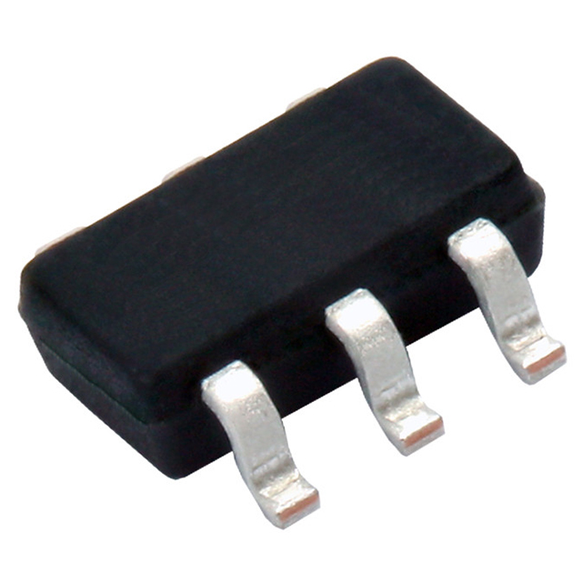
FDC3535 Equivalent & Substitute Parts
Part Overview
The FDC3535 is a P-Channel 80V MOSFET manufactured by onsemi, designed for surface mount applications in the SuperSOT-6 package. This device delivers 2.1A continuous drain current at 25°C with a maximum on-resistance of 183mOhm at rated conditions. The FDC3535 is classified as obsolete, necessitating identification of functionally equivalent alternatives for ongoing design support and procurement continuity. Substitute parts must maintain electrical compatibility across voltage ratings, current handling, and thermal characteristics while accommodating package variations.
Substiute Parts
Key Parameters
| Parameter | Value | Unit |
|---|---|---|
| FET Type | P-Channel | — |
| Drain to Source Voltage (Vdss) | 80 | V |
| Current - Continuous Drain (Id) @ 25°C | 2.1 | A (Ta) |
| Rds On (Max) @ Id, Vgs | 183 | mOhm @ 2.1A, 10V |
| Vgs(th) (Max) @ Id | 3 | V @ 250µA |
| Gate Charge (Qg) (Max) @ Vgs | 20 | nC @ 10V |
| Power Dissipation (Max) | 1.6 | W (Ta) |
| Operating Temperature Range | -55 to 150 | °C (TJ) |
| Package Type | SOT-23-6 Thin, TSOT-23-6 | — |
| RoHS Status | ROHS3 Compliant | — |
Substitute Part Grouping Explanation
Substitution of the FDC3535 is determined by strict equivalence across the following electrical and mechanical parameters:
Electrical Compatibility Criteria:
- FET Type: P-Channel topology required
- Drain to Source Voltage (Vdss): 80V minimum rating
- Continuous Drain Current (Id): Must equal or exceed 2.1A at 25°C
- On-Resistance (Rds On): Must not exceed 183mOhm at specified gate voltage and current
- Gate Threshold Voltage (Vgs(th)): Maximum 3V at 250µA
- Gate Charge (Qg): Maximum 20nC at 10V gate voltage
- Vgs Maximum Rating: ±20V
- Operating Temperature Range: -55°C to 150°C (TJ)
Mechanical & Compliance Criteria:
- Mounting Type: Surface Mount
- Package Compatibility: SOT-23-6 Thin or TSOT-23-6 footprint
- RoHS Status: ROHS3 Compliant
- Moisture Sensitivity Level: MSL 1 (Unlimited)
The SI3129DV-T1-GE3 meets all substitution criteria with enhanced performance characteristics in current handling and thermal dissipation.
Parameter Comparison
| Parameter | FDC3535 (onsemi) | SI3129DV-T1-GE3 (Vishay Siliconix) | Unit |
|---|---|---|---|
| FET Type | P-Channel | P-Channel | — |
| Drain to Source Voltage (Vdss) | 80 | 80 | V |
| Current - Continuous Drain (Id) @ 25°C | 2.1 (Ta) | 3.8 (Ta), 5.4 (Tc) | A |
| Rds On (Max) @ Id, Vgs | 183 @ 2.1A, 10V | 82.7 @ 3.8A, 10V | mOhm |
| Vgs(th) (Max) @ Id | 3 @ 250µA | 2.5 @ 250µA | V |
| Gate Charge (Qg) (Max) @ Vgs | 20 @ 10V | 18 @ 10V | nC |
| Vgs (Max) | ±20 | ±20 | V |
| Input Capacitance (Ciss) (Max) @ Vds | 880 @ 40V | 805 @ 40V | pF |
| Power Dissipation (Max) | 1.6 (Ta) | 2 (Ta), 4.2 (Tc) | W |
| Operating Temperature Range | -55 to 150 | -55 to 150 | °C (TJ) |
| Package Type | SOT-23-6 Thin, TSOT-23-6 | SOT-23-6 Thin, TSOT-23-6 | — |
| RoHS Status | ROHS3 Compliant | ROHS3 Compliant | — |
| Moisture Sensitivity Level (MSL) | 1 (Unlimited) | 1 (Unlimited) | — |
| Product Status | Obsolete | Active | — |
Engineering Selection Recommendations
The SI3129DV-T1-GE3 serves as a direct functional substitute for the obsolete FDC3535. Both devices share identical voltage ratings (80V Vdss), compatible package footprints (SOT-23-6 Thin / TSOT-23-6), and equivalent operating temperature ranges (-55°C to 150°C). Both maintain ROHS3 compliance and MSL 1 moisture sensitivity classification.
The SI3129DV-T1-GE3 demonstrates superior electrical performance: continuous drain current of 3.8A at 25°C (Ta) exceeds the FDC3535's 2.1A specification, and on-resistance of 82.7mOhm at rated conditions is substantially lower than the FDC3535's 183mOhm. Gate threshold voltage is reduced to 2.5V, and gate charge is minimized to 18nC. These improvements result in reduced power dissipation and enhanced thermal performance (4.2W at Tc versus 1.6W at Ta for the original device).
The SI3129DV-T1-GE3 maintains active product status, ensuring long-term availability and supply chain continuity. Both devices are classified under ECCN EAR99 and HTSUS 8541.29.0095, confirming regulatory equivalence for export and trade purposes.
Frequently Asked Questions (FAQ)
Q: Can the SI3129DV-T1-GE3 directly replace the FDC3535 without circuit modification?
A: Yes. Both devices are P-Channel MOSFETs with identical 80V Vdss ratings, compatible SOT-23-6 Thin / TSOT-23-6 package footprints, and matching ±20V gate voltage ratings. The SI3129DV-T1-GE3 exceeds the FDC3535's electrical specifications, making it a direct functional substitute. No circuit redesign is required.
Q: What are the key electrical differences between these parts?
A: The SI3129DV-T1-GE3 provides higher continuous drain current (3.8A at Ta versus 2.1A), lower on-resistance (82.7mOhm versus 183mOhm at rated conditions), lower gate threshold voltage (2.5V versus 3V), and reduced gate charge (18nC versus 20nC). These differences result in improved efficiency and thermal performance while maintaining full voltage and temperature compatibility.
Q: Are the package footprints identical?
A: Both devices use SOT-23-6 Thin and TSOT-23-6 package designations. The physical footprints are compatible, allowing direct PCB layout substitution without modification.
Q: What is the significance of the FDC3535 being obsolete?
A: Obsolete status indicates the FDC3535 is no longer manufactured by onsemi and will not be restocked. The SI3129DV-T1-GE3 maintains active product status with confirmed ongoing availability, ensuring reliable procurement for new designs and production continuity.
Q: Do both parts meet the same compliance standards?
A: Yes. Both the FDC3535 and SI3129DV-T1-GE3 are ROHS3 compliant, carry MSL 1 (Unlimited) moisture sensitivity classification, and are classified under identical ECCN (EAR99) and HTSUS (8541.29.0095) codes. Regulatory and environmental compliance is equivalent.
Q: How do the thermal characteristics compare?
A: The SI3129DV-T1-GE3 demonstrates superior thermal performance with maximum power dissipation of 2W at Ta and 4.2W at Tc, compared to the FDC3535's 1.6W at Ta. The lower on-resistance of the substitute part contributes to reduced power loss in typical operating conditions.
Q: Are there any gate charge or input capacitance considerations for switching applications?
A: The SI3129DV-T1-GE3 exhibits slightly lower gate charge (18nC versus 20nC) and input capacitance (805pF versus 880pF), both measured at equivalent conditions. These reductions may improve switching speed and reduce driver power requirements in high-frequency applications.
Alternative Parts

SJ6012L2TP
Littelfuse Inc.
6 Alternative Parts

JMK107BBJ476MA-RE
Taiyo Yuden
10 Alternative Parts

GMK107BBJ475MA-T
Taiyo Yuden
5 Alternative Parts
SJ6020N2ARP
Littelfuse Inc.
3 Alternative Parts
SJ6025R2ATP
Littelfuse Inc.
4 Alternative Parts

2474-05L
API Delevan Inc.
1 Alternative Parts

4590R-684K
API Delevan Inc.
1 Alternative Parts

CM6560R-334
API Delevan Inc.
1 Alternative Parts

CM6460-104
API Delevan Inc.
1 Alternative Parts

5526-12
API Delevan Inc.
1 Alternative Parts