


Request Quote
(Ships tomorrow)
FDB9409-F085 N-Channel MOSFET 40V 80A Equivalent & Substitute Parts
Part Overview
The FDB9409-F085 is an N-Channel MOSFET manufactured by onsemi, rated for 40V drain-to-source voltage and 80A continuous drain current in a TO-263 (D2PAK) surface mount package. This device is part of the PowerTrench® series and carries automotive-grade qualification (AEC-Q101). The part is currently listed as obsolete, making equivalent and substitute parts necessary for ongoing design support and production continuity. Substitute parts must maintain electrical compatibility across voltage ratings, current handling, gate drive characteristics, and thermal performance while accommodating available packaging options.
Substiute Parts
Key Parameters
| Parameter | FDB9409-F085 | Unit |
|---|---|---|
| Drain-to-Source Voltage (Vdss) | 40 | V |
| Continuous Drain Current @ 25°C (Id) | 80 (Tc) | A |
| On-Resistance @ 80A, 10V (Rds On Max) | 3.5 | mOhm |
| Gate Threshold Voltage @ 250µA (Vgs(th) Max) | 4 | V |
| Gate Charge @ 10V (Qg Max) | 56 | nC |
| Input Capacitance @ 25V (Ciss Max) | 2980 | pF |
| Power Dissipation (Tj) | 94 | W |
| Operating Temperature Range | -55 to 175 | °C |
| Package Type | TO-263 (D2PAK) | — |
| Mounting Type | Surface Mount | — |
| Grade | Automotive | — |
| Qualification | AEC-Q101 | — |
Substitute Part Grouping Explanation
Substitution of the FDB9409-F085 is determined by the following critical electrical and mechanical parameters:
Electrical Compatibility Requirements:
- Drain-to-Source Voltage (Vdss): Must equal or exceed 40V
- Continuous Drain Current (Id): Must meet or exceed 80A at Tc
- On-Resistance (Rds On): Must not exceed 3.5 mOhm at rated current and 10V gate drive
- Gate Threshold Voltage (Vgs(th)): Must be compatible with 10V drive voltage
- Gate Charge (Qg): Lower values reduce switching losses; higher values acceptable if drive circuitry supports
- Input Capacitance (Ciss): Higher values increase gate drive requirements
- Power Dissipation: Must support thermal requirements of the application
- Operating Temperature Range: Must span -55°C to 175°C
Mechanical Compatibility Requirements:
- Package Type: TO-263 variants (D2PAK, TO-263-3, TO-263-7) are acceptable
- Mounting Type: Surface mount only
- Lead Configuration: Pin-compatible or functionally equivalent
Compliance Requirements:
- RoHS3 Compliance: Required
- Automotive Grade: AEC-Q101 qualification preferred for automotive applications
- Moisture Sensitivity Level: MSL 1 (Unlimited) preferred
Substitute parts are grouped into two categories: Direct Package Equivalents (TO-263 variants with matching pinout) and Alternative Package Options (different surface mount packages with equivalent electrical performance).
Parameter Comparison
| Parameter | FDB9409-F085 | DMTH4004SCTB-13 | IPB100N04S204ATMA4 | IXTA220N04T2-7 | 2SK3943-ZP-E1-AY | NVMFS5C450NAFT1G | SUM110N04-04-E3 | Unit |
|---|---|---|---|---|---|---|---|---|
| Manufacturer | onsemi | Diodes Inc. | Infineon | IXYS | Renesas | onsemi | Vishay | — |
| Vdss | 40 | 40 | 40 | 40 | 40 | 40 | 40 | V |
| Id (Tc) | 80 | 100 | 100 | 220 | 82 | 102 | 110 | A |
| Rds On Max @ 10V | 3.5 | 3.0 | 3.3 | 3.5 | 3.5 | 3.3 | 3.5 | mOhm |
| Vgs(th) Max @ 250µA | 4 | 4 | 4 | 4 | — | 3.5 | 4 | V |
| Qg Max @ 10V | 56 | 68.6 | 172 | 112 | 93 | 23 | 200 | nC |
| Ciss Max @ 25V | 2980 | 4305 | 5300 | 6820 | 5800 | 1600 | 6800 | pF |
| Power Dissipation (Tc) | 94 | 136 | 300 | 360 | 104 | 68 | 250 | W |
| Operating Temp Range | -55 to 175 | -55 to 175 | -55 to 175 | -55 to 175 | — | -55 to 175 | -55 to 175 | °C |
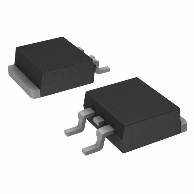
| Package | TO-263 (D2PAK) | TO-263 | PG-TO263-3-2 | TO-263-7 (IXTA) | TO-263 | 5-DFN (5x6) | TO-263 (D2PAK) | — |
| Product Status | Obsolete | Active | Active | Active | Active | Active | Active | — |
| AEC-Q101 | Yes | Yes | Yes | Yes | Yes | Yes | Yes | — |
| RoHS3 | Yes | Yes | Yes | Yes | Yes | Yes | Yes | — |
Engineering Selection Recommendations
Direct Package Equivalents (TO-263 Variants):
The following parts maintain TO-263 package compatibility and are suitable for direct substitution in existing PCB layouts:
DMTH4004SCTB-13 (Diodes Incorporated) — Recommended for applications requiring minimal design changes. This part exceeds the FDB9409-F085 in continuous drain current (100A vs. 80A) and power dissipation (136W vs. 94W) while maintaining identical Vdss, gate threshold voltage, and on-resistance specifications. Active product status with AEC-Q101 qualification and RoHS3 compliance. Available in tape and reel packaging.
IPB100N04S204ATMA4 (Infineon OptiMOS™) — Suitable for applications with higher thermal requirements. Rated for 100A continuous drain current and 300W power dissipation. On-resistance of 3.3 mOhm provides improved efficiency. Higher gate charge (172 nC) and input capacitance (5300 pF) require gate drive circuit verification. Active product status with full automotive qualification.
2SK3943-ZP-E1-AY (Renesas Electronics) — Direct TO-263 package equivalent with 82A continuous drain current and 104W power dissipation. Maintains 3.5 mOhm on-resistance and 4V gate threshold voltage. Higher gate charge (93 nC) and input capacitance (5800 pF) compared to FDB9409-F085. Active product status with AEC-Q101 qualification. Operating temperature range specification incomplete in provided data.
SUM110N04-04-E3 (Vishay TrenchFET®) — TO-263 (D2PAK) package equivalent with 110A continuous drain current and 250W power dissipation. Maintains 3.5 mOhm on-resistance and 4V gate threshold voltage. Significantly higher gate charge (200 nC) and input capacitance (6800 pF) require gate drive circuit evaluation. Active product status with AEC-Q101 qualification and RoHS3 compliance.
Alternative Package Options:
IXTA220N04T2-7 (IXYS TrenchT2™) — TO-263-7 (IXTA) package variant with 6 leads plus tab. Rated for 220A continuous drain current and 360W power dissipation. Maintains 3.5 mOhm on-resistance and 4V gate threshold voltage. Requires PCB layout modification due to different pinout. Active product status with full automotive qualification.
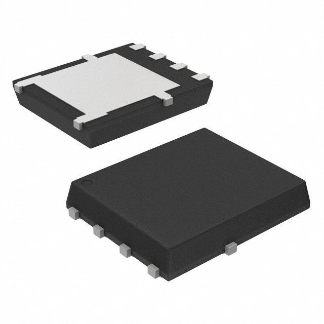
NVMFS5C450NAFT1G (onsemi) — Alternative package in 5-DFN (5x6) format. Rated for 102A continuous drain current (Tc) and 68W power dissipation (Tc). Lowest gate charge (23 nC) and input capacitance (1600 pF) among substitutes, reducing gate drive requirements. Requires significant PCB redesign. Active product status with AEC-Q101 qualification. Available in tape and reel packaging.
Selection Criteria:
- Minimal PCB Modification: Select DMTH4004SCTB-13, 2SK3943-ZP-E1-AY, or SUM110N04-04-E3
- Highest Current Capability: Select IXTA220N04T2-7
- Lowest Gate Drive Requirements: Select NVMFS5C450NAFT1G
- Highest Power Dissipation Capability: Select IXTA220N04T2-7 or IPB100N04S204ATMA4
- Automotive Applications: All listed substitutes carry AEC-Q101 qualification
All substitute parts maintain RoHS3 compliance, MSL 1 moisture sensitivity level, and -55°C to 175°C operating temperature range (where specified).
Frequently Asked Questions (FAQ)
Q: Can I use DMTH4004SCTB-13 as a direct replacement for FDB9409-F085 without PCB modifications?
A: Yes. Both parts use TO-263 (D2PAK) packaging with identical pinout (2 leads plus tab). The DMTH4004SCTB-13 exceeds FDB9409-F085 specifications in current rating (100A vs. 80A) and power dissipation (136W vs. 94W) while maintaining equivalent on-resistance (3.0 mOhm vs. 3.5 mOhm) and gate threshold voltage (4V). No circuit modifications are required.
Q: What is the difference between TO-263 and TO-263-7 packages?
A: TO-263 (D2PAK) contains 3 leads (2 signal leads plus 1 tab for thermal connection). TO-263-7 (IXTA) contains 7 leads (6 signal leads plus 1 tab), providing additional connection points for parallel operation or improved thermal management. TO-263-7 devices require different PCB layouts and cannot be used in TO-263 footprints.
Q: Why does NVMFS5C450NAFT1G have lower gate charge than FDB9409-F085?
A: Gate charge is determined by die size, process technology, and internal circuit design. The NVMFS5C450NAFT1G uses a 5-DFN package with optimized internal geometry, resulting in 23 nC gate charge versus 56 nC for FDB9409-F085. Lower gate charge reduces switching losses and gate drive power consumption but requires PCB redesign due to different package format.
Q: Are all substitute parts automotive-qualified?
A: Yes. All listed substitute parts carry AEC-Q101 automotive qualification, matching the FDB9409-F085 grade. This qualification ensures compliance with automotive reliability and environmental testing standards.
Q: What does "Tc" mean in the continuous drain current specification?
A: "Tc" denotes the current rating at case temperature (typically 25°C). This is the maximum continuous drain current the device can handle under specified thermal conditions. Actual current capability depends on junction temperature, which is influenced by power dissipation and thermal management.
Q: Can I substitute a part with higher gate charge without circuit modifications?
A: Gate charge affects switching speed and gate drive power requirements. Parts with higher gate charge (such as SUM110N04-04-E3 at 200 nC) require gate drive circuits capable of supplying sufficient current to charge the gate within acceptable switching times. Verify gate driver specifications before substitution.
Q: What is the significance of input capacitance (Ciss) in MOSFET selection?
A: Input capacitance affects gate drive circuit design and switching performance. Higher Ciss values (such as 6800 pF in SUM110N04-04-E3) require gate drivers with higher current capability to achieve the same switching speed as devices with lower Ciss. This impacts power dissipation in the gate drive circuit.
Q: Is the NVMFS5C450NAFT1G suitable for high-current applications?
A: The NVMFS5C450NAFT1G is rated for 102A continuous drain current (Tc), exceeding the FDB9409-F085 (80A). However, its 5-DFN package has lower thermal dissipation capability (68W Tc) compared to TO-263 packages (94W to 360W). Use this part only in applications where the 5-DFN thermal performance is adequate for the circuit's power dissipation requirements.
Q: What is the difference between "Ta" and "Tc" temperature ratings?
A: "Ta" denotes ambient temperature rating, while "Tc" denotes case temperature rating. Case temperature is typically higher than ambient temperature due to internal power dissipation. Specifications at Tc represent worst-case performance under elevated thermal conditions.
Q: Can I use IPB100N04S204ATMA4 in a circuit designed for FDB9409-F085?
A: Yes, with gate drive circuit verification. The IPB100N04S204ATMA4 maintains electrical compatibility (40V Vdss, 100A Id, 3.3 mOhm Rds On, 4V Vgs(th)). However, its significantly higher gate charge (172 nC vs. 56 nC) and input capacitance (5300 pF vs. 2980 pF) require gate driver capable of supplying higher current. Verify gate driver specifications before implementation.
Q: Are all substitute parts available in the same packaging options as FDB9409-F085?
A: No. FDB9409-F085 is listed without specific packaging notation. DMTH4004SCTB-13, IPB100N04S204ATMA4, and IXTA220N04T2-7 are available in tape and reel or tube packaging. NVMFS5C450NAFT1G is available in tape and reel. Verify packaging availability with suppliers for production requirements.
Alternative Parts

SJ6012L2TP
Littelfuse Inc.
6 Alternative Parts

JMK107BBJ476MA-RE
Taiyo Yuden
10 Alternative Parts

GMK107BBJ475MA-T
Taiyo Yuden
5 Alternative Parts
SJ6020N2ARP
Littelfuse Inc.
3 Alternative Parts
SJ6025R2ATP
Littelfuse Inc.
4 Alternative Parts

2474-05L
API Delevan Inc.
1 Alternative Parts

4590R-684K
API Delevan Inc.
1 Alternative Parts

CM6560R-334
API Delevan Inc.
1 Alternative Parts

CM6460-104
API Delevan Inc.
1 Alternative Parts

5526-12
API Delevan Inc.
1 Alternative Parts