


Request Quote
(Ships tomorrow)
FDB9403L-F085 Equivalent & Substitute Parts
Part Overview
The FDB9403L-F085 is an N-Channel MOSFET manufactured by onsemi, rated for 40V drain-to-source voltage with 110A continuous drain current at 25°C. This device is housed in a TO-263 (D2PAK) surface mount package and is qualified to AEC-Q101 automotive standards. The part is currently classified as obsolete, necessitating identification of functionally equivalent alternatives for ongoing design support and procurement continuity.
Substiute Parts
Key Parameters
| Parameter | Value | Unit |
|---|---|---|
| Drain-to-Source Voltage (Vdss) | 40 | V |
| Continuous Drain Current (Id) @ 25°C | 110 | A (Tc) |
| On-Resistance (Rds On Max) @ 80A, 10V | 1.2 | mOhm |
| Gate Threshold Voltage (Vgs(th) Max) @ 250µA | 3 | V |
| Gate Charge (Qg Max) @ 10V | 245 | nC |
| Power Dissipation (Max) | 333 | W (Tj) |
| Operating Temperature Range | -55 to 175 | °C (TJ) |
| Package Type | TO-263 (D2PAK) | Surface Mount |
| Automotive Qualification | AEC-Q101 | Yes |
Substitute Part Grouping Explanation
Substitution of the FDB9403L-F085 is determined by electrical and mechanical compatibility across the following critical parameters:
Electrical Compatibility Criteria:
- Drain-to-Source Voltage (Vdss): Must equal or exceed 40V
- Continuous Drain Current (Id): Must support the application's current requirements
- On-Resistance (Rds On): Lower values indicate improved efficiency and reduced thermal dissipation
- Gate Threshold Voltage (Vgs(th)): Must be compatible with gate drive circuitry
- Operating Temperature Range: Must encompass -55°C to 175°C (TJ)
Mechanical Compatibility Criteria:
- Package Type: Surface mount configuration
- Mounting footprint: Physical dimensions must accommodate PCB layout constraints
- Automotive Grade: AEC-Q101 qualification required for automotive applications
Compliance Requirements:
- RoHS3 compliance
- Moisture Sensitivity Level (MSL): 1 (Unlimited)
- REACH unaffected status
The NVMFS5C420NLT1G meets the electrical voltage and temperature specifications while maintaining automotive qualification. However, differences in package type, current rating, and thermal characteristics must be evaluated for specific application requirements.
Parameter Comparison
| Parameter | FDB9403L-F085 | NVMFS5C420NLT1G | Unit |
|---|---|---|---|
| Manufacturer | onsemi | onsemi | — |
| FET Type | N-Channel | N-Channel | — |
| Technology | MOSFET (Metal Oxide) | MOSFET (Metal Oxide) | — |
| Drain-to-Source Voltage (Vdss) | 40 | 40 | V |
| Continuous Drain Current (Id) @ 25°C | 110 (Tc) | 45 (Ta), 277 (Tc) | A |
| On-Resistance (Rds On Max) @ 10V | 1.2 @ 80A | 1.0 @ 50A | mOhm |
| Gate Threshold Voltage (Vgs(th) Max) | 3 @ 250µA | 2.2 @ 200µA | V |
| Gate Charge (Qg Max) @ 10V | 245 | 100 | nC |
| Input Capacitance (Ciss Max) @ 20V | 13500 | 7020 | pF |
| Power Dissipation (Max) | 333 (Tj) | 146 (Tc) | W |
| Operating Temperature Range | -55 to 175 | -55 to 175 | °C (TJ) |
| Grade | Automotive | Automotive | — |
| Qualification | AEC-Q101 | AEC-Q101 | — |
| Mounting Type | Surface Mount | Surface Mount | — |
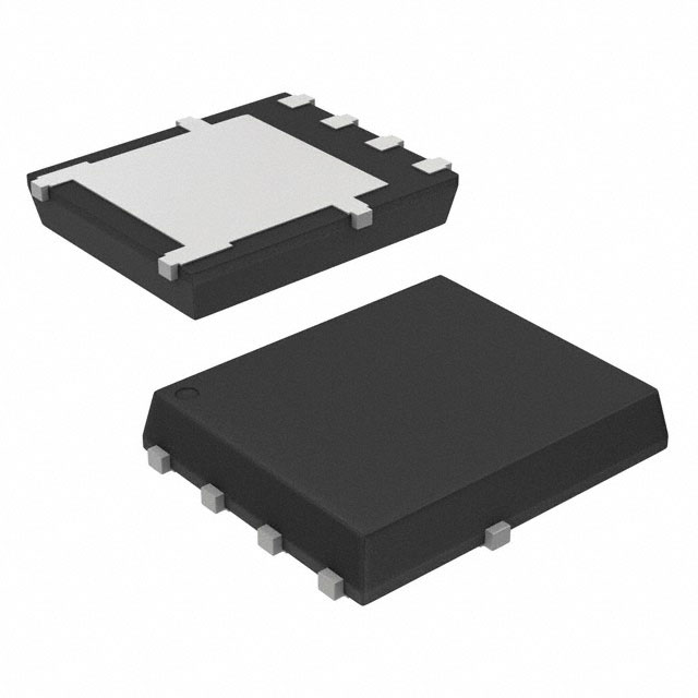
| Package Type | TO-263 (D2PAK) | 5-DFN (5x6) (8-SOFL) | — |
| RoHS Status | ROHS3 Compliant | ROHS3 Compliant | — |
| MSL | 1 (Unlimited) | 1 (Unlimited) | — |
| REACH Status | REACH Unaffected | REACH Unaffected | — |
| Product Status | Obsolete | Active | — |
Engineering Selection Recommendations
Electrical Compatibility: Both devices share identical 40V Vdss ratings and -55°C to 175°C operating temperature ranges, satisfying core voltage and thermal specifications. The NVMFS5C420NLT1G exhibits lower gate charge (100 nC vs. 245 nC) and reduced input capacitance (7020 pF vs. 13500 pF), resulting in faster switching characteristics and reduced gate drive power requirements.
Current Rating Considerations: The FDB9403L-F085 is rated for 110A continuous drain current (Tc). The NVMFS5C420NLT1G provides 277A continuous drain current (Tc), exceeding the original specification. For applications requiring the full 110A rating, the NVMFS5C420NLT1G operates within acceptable margins.
On-Resistance Performance: The NVMFS5C420NLT1G exhibits superior on-resistance characteristics (1.0 mOhm @ 50A, 10V vs. 1.2 mOhm @ 80A, 10V), indicating lower conduction losses and reduced thermal dissipation.
Package and Thermal Considerations: The primary distinction is package type: FDB9403L-F085 uses TO-263 (D2PAK) while NVMFS5C420NLT1G uses 5-DFN (5x6). The TO-263 package provides higher power dissipation capability (333W vs. 146W at Tj). Applications requiring the full 333W dissipation capacity must account for the NVMFS5C420NLT1G's reduced thermal rating through thermal management design modifications.
Compliance and Qualification: Both devices maintain AEC-Q101 automotive qualification, RoHS3 compliance, and MSL 1 (Unlimited) ratings. The NVMFS5C420NLT1G carries active product status, ensuring long-term availability and supply chain continuity.
Frequently Asked Questions (FAQ)
Q: Can the NVMFS5C420NLT1G directly replace the FDB9403L-F085 in existing PCB designs?
A: Direct PCB replacement is not possible due to package differences. The FDB9403L-F085 uses TO-263 (D2PAK) while the NVMFS5C420NLT1G uses 5-DFN (5x6). PCB layout modifications, including footprint redesign and thermal management adjustments, are required.
Q: What are the implications of the lower power dissipation rating in the NVMFS5C420NLT1G?
A: The NVMFS5C420NLT1G is rated for 146W (Tc) compared to 333W (Tj) for the FDB9403L-F085. Applications operating near maximum thermal limits must implement enhanced thermal management, including increased copper area, thermal vias, or external heat sinking, to maintain equivalent thermal performance.
Q: Are both devices suitable for automotive applications?
A: Yes. Both the FDB9403L-F085 and NVMFS5C420NLT1G carry AEC-Q101 automotive qualification and are compliant with RoHS3 and REACH requirements, meeting automotive industry standards.
Q: How do the switching characteristics compare?
A: The NVMFS5C420NLT1G exhibits faster switching due to lower gate charge (100 nC vs. 245 nC) and reduced input capacitance (7020 pF vs. 13500 pF). This results in reduced gate drive power consumption and improved switching speed, beneficial for high-frequency applications.
Q: What is the significance of the different gate threshold voltages?
A: The NVMFS5C420NLT1G has a lower gate threshold voltage (2.2V @ 200µA vs. 3V @ 250µA). This allows operation with lower gate drive voltages, reducing gate drive circuit complexity. Existing gate drive designs must be verified for compatibility with the lower threshold specification.
Q: Is the NVMFS5C420NLT1G available in higher volume quantities?
A: The NVMFS5C420NLT1G carries active product status with documented inventory availability, ensuring consistent supply chain access. The FDB9403L-F085, classified as obsolete, has limited availability and no long-term supply guarantee.
Alternative Parts

SJ6012L2TP
Littelfuse Inc.
6 Alternative Parts

JMK107BBJ476MA-RE
Taiyo Yuden
10 Alternative Parts

GMK107BBJ475MA-T
Taiyo Yuden
5 Alternative Parts
SJ6020N2ARP
Littelfuse Inc.
3 Alternative Parts
SJ6025R2ATP
Littelfuse Inc.
4 Alternative Parts

2474-05L
API Delevan Inc.
1 Alternative Parts

4590R-684K
API Delevan Inc.
1 Alternative Parts

CM6560R-334
API Delevan Inc.
1 Alternative Parts

CM6460-104
API Delevan Inc.
1 Alternative Parts

5526-12
API Delevan Inc.
1 Alternative Parts