


Request Quote
(Ships tomorrow)
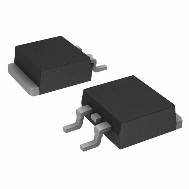
FDB8832 N-Channel MOSFET 30V 34A/80A TO-263 Equivalent & Substitute Parts
Part Overview
The FDB8832 is an N-Channel MOSFET manufactured by onsemi, rated for 30V drain-to-source voltage with continuous drain current of 34A (Ta) and 80A (Tc). The device is housed in a Surface Mount TO-263 (D2PAK) package and features the PowerTrench® technology platform. The FDB8832 is classified as obsolete, necessitating identification of equivalent and substitute components for ongoing design support and procurement requirements. Substitute parts must maintain electrical compatibility across voltage, current, and thermal specifications while preserving the D2PAK package form factor.
Substiute Parts
Key Parameters
| Parameter | FDB8832 Specification |
|---|---|
| Drain-to-Source Voltage (Vdss) | 30 V |
| Continuous Drain Current (Id) @ 25°C | 34A (Ta), 80A (Tc) |
| On-State Resistance (Rds On Max) @ Id, Vgs | 1.9 mOhm @ 80A, 10V |
| Gate Threshold Voltage (Vgs(th) Max) @ Id | 3V @ 250µA |
| Gate Charge (Qg Max) @ Vgs | 265 nC @ 10V |
| Power Dissipation (Max) | 300W (Tc) |
| Operating Temperature Range | -55°C to 175°C (TJ) |
| Package Type | TO-263-3, D2PAK (2 Leads + Tab) |
| Mounting Type | Surface Mount |
| RoHS Status | ROHS3 Compliant |
Substitute Part Grouping Explanation
Substitute parts for the FDB8832 are selected based on strict electrical and mechanical compatibility criteria. The primary substitution parameters are:
Electrical Compatibility Requirements:
- Drain-to-Source Voltage (Vdss): Must equal or exceed 30V
- Continuous Drain Current (Id): Must support 80A (Tc) minimum
- On-State Resistance (Rds On): Lower values indicate improved performance; values within the range of 1.9 mOhm to 4 mOhm are acceptable
- Gate Threshold Voltage: Must be compatible with 3V to 10V gate drive circuits
- Power Dissipation: Must support 300W (Tc) thermal requirements
- Operating Temperature: Must span -55°C to 175°C minimum
Mechanical Compatibility Requirements:
- Package: D2PAK (TO-263-3) form factor required for PCB layout compatibility
- Mounting: Surface Mount technology
- Lead Configuration: 2 Leads + Tab standard
Regulatory Compliance:
- RoHS3 Compliance required
- REACH Status: REACH Unaffected or Vendor Undefined acceptable
Substitute parts are classified into two categories: Upgrade (direct replacement with equal or superior specifications) and Similar (compatible but with parameter variations requiring application review).
Parameter Comparison
| Parameter | FDB8832 (onsemi) | STB80NF03L-04T4 (STMicroelectronics) - Upgrade | SUM90N03-2M2P-E3 (Vishay) - Similar | PHB66NQ03LT (Nexperia) - Similar |
|---|---|---|---|---|
| Manufacturer | onsemi | STMicroelectronics | Vishay Siliconix | Nexperia USA Inc. |
| Drain-to-Source Voltage (Vdss) | 30V | 30V | 30V | 25V |
| Continuous Drain Current (Id) @ 25°C (Tc) | 80A | 80A | 90A | 66A |
| On-State Resistance (Rds On Max) | 1.9 mOhm @ 80A, 10V | 4 mOhm @ 40A, 10V | 2.2 mOhm @ 32A, 10V | 10.5 mOhm @ 25A, 10V |
| Gate Threshold Voltage (Vgs(th) Max) @ Id | 3V @ 250µA | 1V @ 250µA | 2.5V @ 250µA | 2V @ 1mA |
| Gate Charge (Qg Max) @ Vgs | 265 nC @ 10V | 110 nC @ 4.5V | 257 nC @ 10V | 12 nC @ 5V |
| Power Dissipation (Max) | 300W (Tc) | 300W (Tc) | 250W (Tc) | 93W (Tc) |
| Operating Temperature Range | -55°C to 175°C | -60°C to 175°C | -55°C to 175°C | -55°C to 175°C |
| Package Type | TO-263-3, D2PAK | D2PAK | TO-263 (D2PAK) | D2PAK |
| Product Status | Obsolete | Obsolete | Active | Obsolete |
| RoHS Status | ROHS3 Compliant | ROHS3 Compliant | ROHS3 Compliant | ROHS3 Compliant |
Engineering Selection Recommendations
STB80NF03L-04T4 (STMicroelectronics) - Upgrade Classification
The STB80NF03L-04T4 is designated as an upgrade substitute for the FDB8832. Both devices share identical Vdss (30V) and Id (80A) ratings, matching power dissipation capacity (300W Tc), and D2PAK package configuration. The STB80NF03L-04T4 operates across an extended lower temperature range (-60°C minimum versus -55°C), providing additional thermal margin. The device is ROHS3 compliant and carries obsolete product status. Gate charge is reduced (110 nC versus 265 nC), resulting in lower switching losses. The STB80NF03L-04T4 is available in higher inventory quantities (18,839 pcs), supporting procurement continuity.
SUM90N03-2M2P-E3 (Vishay Siliconix) - Similar Classification
The SUM90N03-2M2P-E3 is classified as a similar substitute with enhanced current capability (90A versus 80A). Vdss matches at 30V, and operating temperature range aligns with the FDB8832 (-55°C to 175°C). On-state resistance is superior (2.2 mOhm versus 1.9 mOhm), and gate charge is comparable (257 nC versus 265 nC). Power dissipation is rated at 250W (Tc), which is 50W lower than the FDB8832. The SUM90N03-2M2P-E3 maintains active product status, ensuring long-term availability and technical support. ROHS3 compliance is confirmed. This device is suitable for applications requiring higher current capacity within the same voltage class.
PHB66NQ03LT (Nexperia USA Inc.) - Similar Classification
The PHB66NQ03LT is classified as a similar substitute with reduced voltage and current ratings. Vdss is limited to 25V (5V lower than FDB8832), and continuous drain current is 66A (14A lower than FDB8832). Power dissipation is significantly reduced to 93W (Tc), representing a 207W reduction from the FDB8832 specification. Gate charge is substantially lower (12 nC versus 265 nC), indicating reduced switching losses. Operating temperature range matches the FDB8832 (-55°C to 175°C). ROHS3 compliance is confirmed. This device is applicable only to applications with reduced voltage and power requirements.
Frequently Asked Questions (FAQ)
Q: Can the STB80NF03L-04T4 directly replace the FDB8832 in existing designs?
A: Yes. The STB80NF03L-04T4 is electrically and mechanically compatible with the FDB8832. Both devices share identical Vdss (30V), Id (80A), power dissipation (300W Tc), and D2PAK package configuration. Gate drive voltage compatibility is maintained across the 4.5V to 10V range. No circuit modifications are required for direct substitution.
Q: What is the primary difference between the STB80NF03L-04T4 and SUM90N03-2M2P-E3?
A: The STB80NF03L-04T4 matches the FDB8832 specifications exactly (30V, 80A, 300W), while the SUM90N03-2M2P-E3 offers higher current capability (90A) but reduced power dissipation (250W Tc). The SUM90N03-2M2P-E3 maintains active product status, whereas the STB80NF03L-04T4 is obsolete. Selection depends on application current requirements and long-term availability needs.
Q: Is the PHB66NQ03LT suitable as a substitute for the FDB8832?
A: The PHB66NQ03LT is not a direct substitute. It operates at reduced voltage (25V versus 30V) and current (66A versus 80A) ratings, with significantly lower power dissipation (93W versus 300W). This device is applicable only to applications with lower voltage and power requirements that do not exceed 25V operation.
Q: Are all substitute parts RoHS3 compliant?
A: Yes. The FDB8832, STB80NF03L-04T4, SUM90N03-2M2P-E3, and PHB66NQ03LT are all ROHS3 compliant, meeting environmental and regulatory requirements for lead-free manufacturing and hazardous substance restrictions.
Q: What is the significance of product status (Obsolete versus Active)?
A: Product status indicates manufacturer support and long-term availability. The FDB8832, STB80NF03L-04T4, and PHB66NQ03LT are obsolete, meaning manufacturing has been discontinued. The SUM90N03-2M2P-E3 maintains active status, ensuring continued production, technical documentation updates, and supplier support. For new designs, active-status components are preferred; for legacy system support, obsolete components may be sourced from inventory.
Q: Do all substitute parts use the same D2PAK package?
A: Yes. The FDB8832, STB80NF03L-04T4, SUM90N03-2M2P-E3, and PHB66NQ03LT all use the D2PAK (TO-263-3) Surface Mount package with 2 Leads + Tab configuration. PCB layout and thermal management designs are directly compatible across all four devices.
Q: What gate drive voltage is required for these MOSFETs?
A: All substitute parts operate with gate drive voltages in the 4.5V to 10V range. The FDB8832 specifies maximum on-state resistance at 10V gate drive. The STB80NF03L-04T4 and SUM90N03-2M2P-E3 also specify performance at 10V. Existing gate drive circuits designed for the FDB8832 are compatible with all substitute parts.
Q: How does on-state resistance affect device selection?
A: On-state resistance (Rds On) directly impacts power dissipation and thermal performance. Lower Rds On values reduce conduction losses. The FDB8832 specifies 1.9 mOhm (best performance), SUM90N03-2M2P-E3 specifies 2.2 mOhm (comparable), STB80NF03L-04T4 specifies 4 mOhm (higher losses), and PHB66NQ03LT specifies 10.5 mOhm (significantly higher losses). Applications with stringent thermal budgets should prioritize lower Rds On values.
Q: What is gate charge and why does it matter?
A: Gate charge (Qg) represents the total charge required to switch the MOSFET from off to on state. Higher gate charge increases switching losses and requires higher gate drive current. The FDB8832 specifies 265 nC, while the STB80NF03L-04T4 specifies 110 nC (lower switching losses). For high-frequency switching applications, lower gate charge reduces power consumption and heat generation.
Alternative Parts

SJ6012L2TP
Littelfuse Inc.
6 Alternative Parts

JMK107BBJ476MA-RE
Taiyo Yuden
10 Alternative Parts

GMK107BBJ475MA-T
Taiyo Yuden
5 Alternative Parts
SJ6020N2ARP
Littelfuse Inc.
3 Alternative Parts
SJ6025R2ATP
Littelfuse Inc.
4 Alternative Parts

2474-05L
API Delevan Inc.
1 Alternative Parts

4590R-684K
API Delevan Inc.
1 Alternative Parts

CM6560R-334
API Delevan Inc.
1 Alternative Parts

CM6460-104
API Delevan Inc.
1 Alternative Parts

5526-12
API Delevan Inc.
1 Alternative Parts