


Request Quote
(Ships tomorrow)
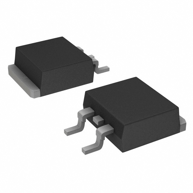
FDB5645 N-Channel MOSFET Equivalent & Substitute Parts
Part Overview
The FDB5645 is an N-Channel MOSFET manufactured by onsemi, rated for 60V drain-to-source voltage and 80A continuous drain current in a surface mount TO-263 (D2PAK) package. This device is part of the PowerTrench® series and is classified as obsolete. Due to its obsolete status, equivalent and substitute parts from active manufacturers are necessary to maintain design continuity and ensure long-term component availability for new production and field replacements.
Substiute Parts
Key Parameters
| Parameter | FDB5645 Value | Unit |
|---|---|---|
| Drain-to-Source Voltage (Vdss) | 60 | V |
| Continuous Drain Current (Id) @ 25°C | 80 | A (Ta) |
| On-State Resistance (Rds On) @ 40A, 10V | 9.5 | mOhm |
| Gate Threshold Voltage (Vgs(th)) @ 250µA | 4 | V |
| Gate Charge (Qg) @ 10V | 107 | nC |
| Input Capacitance (Ciss) @ 30V | 4468 | pF |
| Power Dissipation (Tc) | 125 | W |
| Operating Temperature Range | -65 to 175 | °C (TJ) |
| Package Type | TO-263 (D2PAK) | Surface Mount |
| FET Type | N-Channel | MOSFET |
Substitute Part Grouping Explanation
Substitution of the FDB5645 is determined by the following critical electrical and mechanical parameters:
Primary Substitution Criteria:
- Drain-to-Source Voltage (Vdss): Must be equal to or greater than 60V
- Continuous Drain Current (Id): Must be equal to or greater than 80A
- Package Type: Must be TO-263 (D2PAK) surface mount
- FET Type: Must be N-Channel MOSFET
- On-State Resistance (Rds On): Should be comparable to enable equivalent thermal and switching performance
Secondary Compatibility Factors:
- Gate Threshold Voltage (Vgs(th)): Acceptable range 2.2V to 4V
- Maximum Gate Voltage (Vgs Max): Must support ±20V operation
- Operating Temperature Range: Must encompass -55°C to 175°C minimum
- Moisture Sensitivity Level (MSL): Level 1 or 3 acceptable for most applications
Substitute parts are grouped into three categories based on voltage and current ratings:
- Direct Equivalents (60V, 80A+): Parts matching or exceeding both voltage and current specifications with comparable Rds On values
- Lower Voltage Alternatives (55V, 80A+): Parts with reduced voltage rating but maintained or increased current capacity
- Reduced Current Alternatives (60V, 50-75A): Parts with maintained voltage but lower current ratings for lower-power applications
Parameter Comparison
| Part Number | Manufacturer | Vdss (V) | Id (A) | Rds On (mOhm) | Qg (nC) | Ciss (pF) | Pd (W) | Status | Package |
|---|---|---|---|---|---|---|---|---|---|
| FDB5645 | onsemi | 60 | 80 (Ta) | 9.5 @ 40A, 10V | 107 @ 10V | 4468 @ 30V | 125 (Tc) | Obsolete | TO-263 (D2PAK) |
| IPB081N06L3GATMA1 | Infineon | 60 | 50 (Tc) | 8.1 @ 50A, 10V | 29 @ 4.5V | 4900 @ 30V | 79 (Tc) | Active | TO-263 (D2PAK) |
| IPB090N06N3GATMA1 | Infineon | 60 | 50 (Tc) | 9 @ 50A, 10V | 36 @ 10V | 2900 @ 30V | 71 (Tc) | Active | TO-263 (D2PAK) |
| IPB80N06S209ATMA2 | Infineon | 55 | 80 (Tc) | 8.8 @ 50A, 10V | 80 @ 10V | 2360 @ 25V | 190 (Tc) | Active | TO-263 (D2PAK) |
| BUK768R3-60E,118 | Nexperia | 60 | 75 (Tc) | 8.3 @ 20A, 10V | 43.1 @ 10V | 2920 @ 25V | 137 (Tc) | Active | TO-263 (D2PAK) |
| PSMN7R6-60BS,118 | Nexperia | 60 | 92 (Tc) | 7.8 @ 25A, 10V | 38.7 @ 10V | 2651 @ 30V | 149 (Tc) | Active | TO-263 (D2PAK) |
| PSMN015-60BS,118 | Nexperia | 60 | 50 (Tc) | 14.8 @ 15A, 10V | 20.9 @ 10V | 1220 @ 30V | 86 (Tc) | Active | TO-263 (D2PAK) |
| STB141NF55 | STMicroelectronics | 55 | 80 (Tc) | 8 @ 40A, 10V | 142 @ 10V | 5300 @ 25V | 300 (Tc) | Active | TO-263 (D2PAK) |
| IXTA90N055T2 | IXYS | 55 | 90 (Tc) | 8.4 @ 25A, 10V | 42 @ 10V | 2770 @ 25V | 150 (Tc) | Active | TO-263 (D2PAK) |
| IRFS3607TRLPBF | Infineon | 75 | 80 (Tc) | 9 @ 46A, 10V | 84 @ 10V | 3070 @ 50V | 140 (Tc) | Active | TO-263 (D2PAK) |
| AOB470L | Alpha & Omega | 75 | 100 (Tc) | 10.2 @ 30A, 10V | 136 @ 10V | 5640 @ 30V | 268 (Tc) | Active | TO-263 (D2PAK) |
Engineering Selection Recommendations
Category 1: Direct Voltage & Current Match (60V, 80A+)
PSMN7R6-60BS,118 (Nexperia) is the primary substitute for the FDB5645. This part maintains the 60V voltage rating and exceeds the 80A current specification at 92A continuous drain current. The on-state resistance of 7.8 mOhm at 25A, 10V is superior to the FDB5645 specification, resulting in lower power dissipation and improved thermal performance. The part is RoHS3 compliant and carries active product status with full manufacturing support.
Category 2: Matched Current with Reduced Voltage (55V, 80A+)
IPB80N06S209ATMA2 (Infineon) and STB141NF55 (STMicroelectronics) both provide 80A continuous drain current at a reduced 55V rating. The IPB80N06S209ATMA2 offers superior power dissipation capability at 190W (Tc) and lower on-state resistance of 8.8 mOhm. The STB141NF55 provides exceptional power dissipation at 300W (Tc), making it suitable for high-thermal-stress applications. Both are RoHS3 compliant and active products.
IXTA90N055T2 (IXYS) provides 90A continuous drain current at 55V, exceeding the FDB5645 current specification while accepting a 5V voltage reduction. This part is suitable for applications where the 55V rating is acceptable and higher current capacity is beneficial.
Category 3: Matched Voltage with Reduced Current (60V, 50-75A)
BUK768R3-60E,118 (Nexperia) maintains the 60V rating with 75A continuous drain current, providing a near-equivalent substitute for applications with slightly lower current requirements. This part carries AEC-Q101 automotive qualification and is suitable for automotive-grade applications. RoHS3 compliant and active status.
PSMN015-60BS,118 (Nexperia) and IPB081N06L3GATMA1 (Infineon) both provide 50A continuous drain current at 60V. These parts are suitable for lower-power applications or as conservative substitutes where thermal margin is prioritized. Both are RoHS3 compliant and active products.
Category 4: Higher Voltage Alternative (75V, 80A+)
IRFS3607TRLPBF (Infineon) and AOB470L (Alpha & Omega) both provide 75V voltage rating with 80A or greater continuous drain current. These parts are suitable for applications requiring higher voltage headroom. IRFS3607TRLPBF maintains 80A at 75V with 9 mOhm on-state resistance. AOB470L provides 100A continuous drain current at 75V, offering significant current margin. Both are RoHS3 compliant and active products.
Compliance & Certification:
All recommended substitute parts are RoHS3 compliant except where noted. All parts maintain REACH Unaffected status and EAR99 export classification consistent with the FDB5645. Moisture Sensitivity Level is 1 (Unlimited) for all active substitutes except STB141NF55, which carries MSL 3 (168 Hours).
Frequently Asked Questions (FAQ)
Q: Can I use a 55V-rated MOSFET as a direct replacement for the 60V FDB5645?
A: A 55V-rated MOSFET can be used only if the application circuit operates at voltages below 55V. The reduced voltage rating provides less safety margin against voltage transients and overshoot conditions. Parts such as IPB80N06S209ATMA2, STB141NF55, and IXTA90N055T2 are suitable only for applications where the maximum drain-to-source voltage does not exceed 55V under any operating condition, including transient events.
Q: What is the significance of on-state resistance (Rds On) when selecting a substitute?
A: On-state resistance directly determines power dissipation and thermal performance. Lower Rds On values result in reduced heat generation at the same current level. The FDB5645 specifies 9.5 mOhm at 40A, 10V. Substitute parts with lower Rds On values (such as PSMN7R6-60BS,118 at 7.8 mOhm) provide improved efficiency and reduced thermal stress. Higher Rds On values require verification that the application's thermal design can accommodate increased power dissipation.
Q: Are all substitute parts pin-compatible with the FDB5645?
A: Yes. All substitute parts listed use the TO-263 (D2PAK) package with identical pin configuration: Gate, Drain, and Source connections. Physical dimensions and PCB footprints are standardized across all TO-263 variants. No PCB modifications are required for package compatibility.
Q: What is the difference between Ta and Tc current ratings?
A: Ta (ambient temperature) current rating is measured at 25°C ambient temperature without active cooling. Tc (case temperature) current rating is measured at a specified case temperature, typically 25°C, and represents the maximum current the device can handle with proper thermal management. The FDB5645 specifies 80A (Ta), indicating this is the ambient-temperature rating. Substitute parts often specify Tc ratings, which may be higher due to improved thermal design. When comparing current ratings, ensure both specifications use the same temperature reference.
Q: Can I use a higher-current-rated MOSFET as a substitute?
A: Yes. A MOSFET with higher current rating (such as AOB470L at 100A versus FDB5645 at 80A) is a valid substitute provided all other parameters meet or exceed the original specification. Higher current rating provides additional design margin and typically indicates improved thermal characteristics. No circuit modifications are required.
Q: What does RoHS3 compliance mean for component selection?
A: RoHS3 compliance indicates the part meets Restriction of Hazardous Substances Directive requirements, restricting lead, cadmium, mercury, and other hazardous materials. All active substitute parts listed are RoHS3 compliant, ensuring compatibility with modern manufacturing and environmental regulations. The obsolete FDB5645 may not carry RoHS3 certification, making active substitutes necessary for new production designs.
Q: Is the gate charge (Qg) parameter important for substitution?
A: Gate charge affects switching speed and gate drive circuit requirements. The FDB5645 specifies 107 nC at 10V. Substitute parts show varying gate charge values (ranging from 20.9 nC to 142 nC). Lower gate charge enables faster switching and reduces gate drive power consumption. Higher gate charge may require verification that the gate drive circuit can supply sufficient current within the required switching time. For most applications, gate charge differences are accommodated by standard gate drive circuits without modification.
Q: What is Moisture Sensitivity Level (MSL) and why does it matter?
A: MSL indicates the maximum time a component can be exposed to moisture at specified temperature and humidity before soldering. MSL 1 (Unlimited) means the part has no moisture sensitivity restrictions. MSL 3 (168 Hours) means the part must be soldered within 168 hours of exposure to 85°C/85% relative humidity. Most substitute parts carry MSL 1. STB141NF55 carries MSL 3, requiring standard moisture-control procedures during storage and handling. This does not affect electrical performance but impacts supply chain and manufacturing logistics.
Q: Can I substitute a part with higher power dissipation rating?
A: Yes. A substitute with higher power dissipation rating (such as STB141NF55 at 300W versus FDB5645 at 125W) indicates improved thermal design and is a valid substitute. Higher power dissipation capability provides additional thermal margin and allows operation at higher currents or ambient temperatures without exceeding junction temperature limits. No circuit modifications are required.
Q: What should I verify before finalizing a substitute part selection?
A: Verify the following parameters match or exceed the FDB5645 specification: (1) Drain-to-Source Voltage (Vdss) ≥ 60V, (2) Continuous Drain Current (Id) ≥ 80A, (3) Package type is TO-263 (D2PAK), (4) Gate Threshold Voltage (Vgs(th)) is within acceptable range (2.2V to 4V), (5) Maximum Gate Voltage (Vgs Max) supports ±20V, (6) Operating temperature range encompasses -55°C to 175°C minimum. Additionally, confirm the gate drive circuit can supply the required gate charge within the specified switching time, and verify the application's thermal design can accommodate the substitute part's power dissipation characteristics.
Alternative Parts

SJ6012L2TP
Littelfuse Inc.
6 Alternative Parts

JMK107BBJ476MA-RE
Taiyo Yuden
10 Alternative Parts

GMK107BBJ475MA-T
Taiyo Yuden
5 Alternative Parts
SJ6020N2ARP
Littelfuse Inc.
3 Alternative Parts
SJ6025R2ATP
Littelfuse Inc.
4 Alternative Parts

2474-05L
API Delevan Inc.
1 Alternative Parts

4590R-684K
API Delevan Inc.
1 Alternative Parts

CM6560R-334
API Delevan Inc.
1 Alternative Parts

CM6460-104
API Delevan Inc.
1 Alternative Parts

5526-12
API Delevan Inc.
1 Alternative Parts