


Request Quote
(Ships tomorrow)
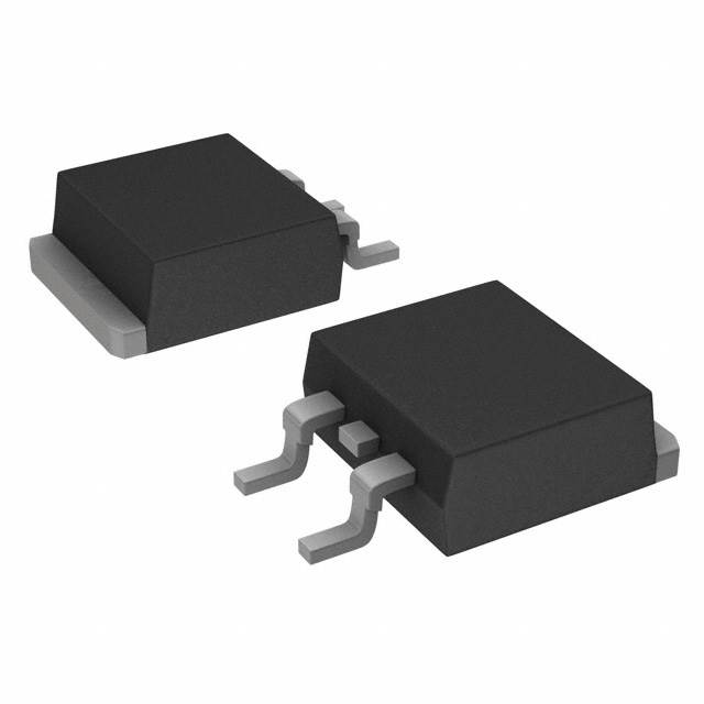
FDB2570 Equivalent & Substitute Parts
Part Overview
The FDB2570 is an N-Channel MOSFET manufactured by onsemi, rated for 150V drain-to-source voltage with 22A continuous drain current in a Surface Mount TO-263 (D2PAK) package. This device is classified as obsolete, necessitating identification of equivalent and substitute components for ongoing design support and procurement continuity. Obsolete status requires engineers to evaluate functionally compatible alternatives that maintain electrical and mechanical compatibility within the application circuit.
Substiute Parts
Key Parameters
| Parameter | Value | Unit |
|---|---|---|
| Drain to Source Voltage (Vdss) | 150 | V |
| Continuous Drain Current (Id) @ 25°C | 22 | A (Ta) |
| Rds On (Max) @ Id, Vgs | 80 mOhm @ 11A, 10V | mOhm |
| Gate Threshold Voltage Vgs(th) (Max) | 4 | V @ 250µA |
| Gate Charge (Qg) (Max) @ Vgs | 56 | nC @ 10V |
| Input Capacitance (Ciss) (Max) | 1911 | pF @ 75V |
| Power Dissipation (Max) | 93 | W (Tc) |
| Operating Temperature Range | -65 to 175 | °C (TJ) |
| Package Type | TO-263-3 (D2PAK) | Surface Mount |
| FET Type | N-Channel | — |
| Technology | MOSFET (Metal Oxide) | — |
Substitute Part Grouping Explanation
Substitution of the FDB2570 is determined by strict electrical and mechanical parameter compatibility. The primary substitution criteria are:
Electrical Compatibility Requirements:
- Drain-to-Source Voltage (Vdss) must equal or exceed 150V
- Continuous Drain Current (Id) must meet or exceed 22A at 25°C
- On-state resistance (Rds On) must not exceed the maximum specified value to prevent thermal runaway
- Gate threshold voltage (Vgs(th)) must remain within compatible switching thresholds
- Gate charge (Qg) and input capacitance (Ciss) must be compatible with existing gate drive circuitry
Mechanical Compatibility Requirements:
- Package type must be TO-263-3 (D2PAK) Surface Mount configuration
- Pin configuration must match the 2 Leads + Tab layout
- Mounting footprint must be identical for direct PCB replacement
Environmental & Compliance Requirements:
- Operating temperature range must support the application's thermal requirements
- Moisture Sensitivity Level (MSL) classification must be compatible with assembly processes
- REACH and ECCN compliance status must meet regulatory requirements
The NTB35N15T4G qualifies as a substitute based on matching Vdss (150V), exceeding Id requirement (37A vs. 22A), maintaining compatible Rds On characteristics (50 mOhm vs. 80 mOhm), and sharing identical D2PAK packaging and pin configuration.
Parameter Comparison
| Parameter | FDB2570 | NTB35N15T4G | Unit |
|---|---|---|---|
| Manufacturer | onsemi | onsemi | — |
| FET Type | N-Channel | N-Channel | — |
| Technology | MOSFET (Metal Oxide) | MOSFET (Metal Oxide) | — |
| Drain to Source Voltage (Vdss) | 150 | 150 | V |
| Continuous Drain Current (Id) @ 25°C | 22 | 37 | A (Ta) |
| Rds On (Max) @ Id, Vgs | 80 @ 11A, 10V | 50 @ 18.5A, 10V | mOhm |
| Gate Threshold Voltage Vgs(th) (Max) | 4 @ 250µA | 4 @ 250µA | V |
| Gate Charge (Qg) (Max) @ Vgs | 56 @ 10V | 100 @ 10V | nC |
| Input Capacitance (Ciss) (Max) | 1911 @ 75V | 3200 @ 25V | pF |
| Power Dissipation (Max) | 93 (Tc) | 178 (Tj) | W |
| Operating Temperature Range | -65 to 175 | -55 to 150 | °C (TJ) |
| Mounting Type | Surface Mount | Surface Mount | — |
| Package Type | TO-263-3 (D2PAK) | TO-263-3 (D2PAK) | — |
| Product Status | Obsolete | Obsolete | — |
| Moisture Sensitivity Level (MSL) | 1 (Unlimited) | 1 (Unlimited) | — |
| REACH Status | REACH Unaffected | REACH Unaffected | — |
| ECCN | EAR99 | EAR99 | — |
Engineering Selection Recommendations
FDB2570 to NTB35N15T4G Substitution:
The NTB35N15T4G is electrically and mechanically compatible with the FDB2570 for direct substitution. Both devices share identical Vdss (150V) and gate threshold voltage specifications (4V @ 250µA), ensuring compatible gate drive requirements. The NTB35N15T4G provides superior current handling capability (37A vs. 22A) and lower on-state resistance (50 mOhm vs. 80 mOhm), resulting in reduced power dissipation and improved thermal performance in the application.
Both components are classified as obsolete and manufactured by onsemi. Both maintain MSL Level 1 (Unlimited) moisture sensitivity classification and REACH Unaffected compliance status, ensuring compatibility with standard assembly and handling procedures. Both carry EAR99 ECCN classification.
Temperature Range Consideration:
The NTB35N15T4G operating temperature range (-55°C to 150°C) is narrower than the FDB2570 (-65°C to 175°C). Applications requiring operation below -55°C or above 150°C must retain the FDB2570 or identify alternative components with extended temperature specifications.
Gate Drive Circuit Impact:
The NTB35N15T4G exhibits higher gate charge (100 nC vs. 56 nC) and input capacitance (3200 pF vs. 1911 pF). Gate drive circuits must supply sufficient current to charge the gate within the required switching time. Existing gate drive designs must be evaluated for compatibility with these increased capacitive loads.
Frequently Asked Questions (FAQ)
Q: Can the NTB35N15T4G directly replace the FDB2570 on the PCB?
A: Yes. Both devices use identical TO-263-3 (D2PAK) Surface Mount packaging with matching pin configurations (2 Leads + Tab). The footprint and pinout are identical, enabling direct PCB replacement without layout modifications.
Q: What are the key electrical differences between these devices?
A: The NTB35N15T4G provides higher continuous drain current (37A vs. 22A) and lower on-state resistance (50 mOhm vs. 80 mOhm). Gate charge and input capacitance are higher in the NTB35N15T4G, requiring gate drive circuit evaluation. Both maintain identical Vdss (150V) and gate threshold voltage (4V @ 250µA).
Q: Are there temperature range limitations with the NTB35N15T4G?
A: Yes. The NTB35N15T4G operates from -55°C to 150°C, compared to the FDB2570 range of -65°C to 175°C. Applications requiring operation below -55°C or above 150°C must use the FDB2570 or identify components with extended temperature specifications.
Q: Do both devices meet the same compliance requirements?
A: Yes. Both the FDB2570 and NTB35N15T4G are REACH Unaffected, carry EAR99 ECCN classification, and maintain MSL Level 1 (Unlimited) moisture sensitivity. Both are classified as obsolete products.
Q: Will the higher gate charge of the NTB35N15T4G affect my circuit?
A: The NTB35N15T4G gate charge (100 nC) is higher than the FDB2570 (56 nC). Gate drive circuits must supply sufficient current to charge the gate within the required switching time. Existing gate drive designs must be evaluated to confirm compatibility with the increased gate charge specification.
Q: What is the impact of lower on-state resistance in the NTB35N15T4G?
A: Lower on-state resistance (50 mOhm vs. 80 mOhm) reduces power dissipation and heat generation during conduction. This improves thermal performance and may reduce cooling requirements in the application. Thermal design margins improve with the NTB35N15T4G.
Q: Are both devices still in production?
A: No. Both the FDB2570 and NTB35N15T4G are classified as obsolete. Procurement must account for limited inventory availability and potential future supply constraints.
Alternative Parts

SJ6012L2TP
Littelfuse Inc.
6 Alternative Parts

JMK107BBJ476MA-RE
Taiyo Yuden
10 Alternative Parts

GMK107BBJ475MA-T
Taiyo Yuden
5 Alternative Parts
SJ6020N2ARP
Littelfuse Inc.
3 Alternative Parts
SJ6025R2ATP
Littelfuse Inc.
4 Alternative Parts

2474-05L
API Delevan Inc.
1 Alternative Parts

4590R-684K
API Delevan Inc.
1 Alternative Parts

CM6560R-334
API Delevan Inc.
1 Alternative Parts

CM6460-104
API Delevan Inc.
1 Alternative Parts

5526-12
API Delevan Inc.
1 Alternative Parts