


Request Quote
(Ships tomorrow)
FCP850N80Z N-Channel MOSFET 800V 8A Equivalent & Substitute Parts
Part Overview
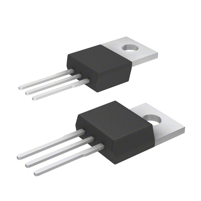
The FCP850N80Z is an N-Channel MOSFET manufactured by onsemi, designed for high-voltage switching applications with a maximum drain-to-source voltage rating of 800V and continuous drain current of 8A at 25°C. This device features the SuperFET® II technology platform and is packaged in a Through Hole TO-220-3 configuration with a maximum power dissipation of 136W.
The FCP850N80Z carries a "Not For New Designs" product status, indicating that onsemi has discontinued active development for this part. This status necessitates identification of functionally equivalent alternatives for ongoing production requirements, maintenance applications, and design continuity where the original specification remains valid.
Substiute Parts
Key Parameters
| Parameter | Value | Unit |
|---|---|---|
| Drain to Source Voltage (Vdss) | 800 | V |
| Continuous Drain Current (Id) @ 25°C | 8 | A |
| Rds On (Max) @ Id, Vgs | 850 mOhm @ 3A, 10V | mOhm |
| Gate Threshold Voltage Vgs(th) (Max) | 4.5 | V @ 600µA |
| Gate Charge (Qg) (Max) @ Vgs | 29 | nC @ 10V |
| Maximum Gate Voltage (Vgs) | ±20 | V |
| Input Capacitance (Ciss) (Max) @ Vds | 1315 | pF @ 100V |
| Power Dissipation (Max) | 136 | W |
| Operating Temperature Range | -55 to 150 | °C |
| Package Type | TO-220-3 | Through Hole |
| RoHS Status | ROHS3 Compliant | - |
Substitute Part Grouping Explanation
Substitution of the FCP850N80Z is evaluated based on the following critical electrical and mechanical parameters:
Voltage Rating Compatibility: The substitute part must support the application's maximum operating voltage. The FCP850N80Z operates at 800V Vdss. Substitute parts with lower voltage ratings (such as 650V) are acceptable only in applications where the actual circuit voltage does not exceed the substitute's rating.
Current Handling Capability: The FCP850N80Z provides 8A continuous drain current. Substitute parts with lower current ratings require verification that the application's maximum current demand does not exceed the substitute's specification.
On-State Resistance (Rds On): The FCP850N80Z specifies 850 mOhm maximum at 3A, 10V. This parameter directly affects power dissipation and thermal performance. Substitute parts with comparable or lower Rds On values maintain equivalent thermal characteristics.
Gate Drive Requirements: Both parts operate with 10V drive voltage for maximum Rds On specification, ensuring compatibility with standard gate driver circuits.
Package and Mounting: The FCP850N80Z uses TO-220-3 Through Hole packaging. Substitute parts must use identical or mechanically compatible packaging to ensure PCB layout compatibility and thermal management effectiveness.
Compliance and Product Status: The FCP850N80Z is ROHS3 compliant and REACH unaffected. Substitute parts must maintain equivalent compliance status for regulated applications.
Parameter Comparison
| Parameter | FCP850N80Z (onsemi) | IXTP4N65X2 (IXYS) | Unit |
|---|---|---|---|
| Drain to Source Voltage (Vdss) | 800 | 650 | V |
| Continuous Drain Current (Id) @ 25°C | 8 | 4 | A |
| Rds On (Max) @ Id, Vgs | 850 @ 3A, 10V | 850 @ 2A, 10V | mOhm |
| Gate Threshold Voltage Vgs(th) (Max) | 4.5 @ 600µA | 5.0 @ 250µA | V |
| Gate Charge (Qg) (Max) @ Vgs | 29 @ 10V | 8.3 @ 10V | nC |
| Maximum Gate Voltage (Vgs) | ±20 | ±30 | V |
| Input Capacitance (Ciss) (Max) @ Vds | 1315 @ 100V | 455 @ 25V | pF |
| Power Dissipation (Max) | 136 | 80 | W |
| Operating Temperature Range | -55 to 150 | -55 to 150 | °C |
| Package Type | TO-220-3 | TO-220-3 | - |
| RoHS Status | ROHS3 Compliant | ROHS3 Compliant | - |
| Product Status | Not For New Designs | Active | - |
Engineering Selection Recommendations
IXTP4N65X2 Substitution Criteria:
The IXTP4N65X2 manufactured by IXYS is an active product with ROHS3 compliance and REACH unaffected status, making it suitable for regulated applications requiring current component availability.
Voltage Derating: The IXTP4N65X2 has a maximum Vdss rating of 650V compared to the FCP850N80Z's 800V. This 150V reduction in voltage rating requires that the application's actual operating voltage remain below 650V. Applications designed for the full 800V capability of the FCP850N80Z cannot use this substitute without circuit redesign.
Current Derating: The IXTP4N65X2 provides 4A continuous drain current versus the FCP850N80Z's 8A. Applications requiring the full 8A capability must implement current derating or parallel device configurations.
On-State Resistance: Both devices specify 850 mOhm maximum Rds On at their respective drive conditions, maintaining equivalent conduction losses at rated current levels.
Gate Charge Reduction: The IXTP4N65X2 exhibits significantly lower gate charge (8.3 nC versus 29 nC), resulting in faster switching transitions and reduced gate driver power requirements.
Power Dissipation: The IXTP4N65X2 is rated for 80W maximum power dissipation compared to 136W for the FCP850N80Z. Thermal management design must account for this reduced dissipation capability.
Compliance Status: Both devices maintain ROHS3 compliance and REACH unaffected status, ensuring regulatory compatibility for equivalent applications.
Frequently Asked Questions (FAQ)
Q: Can the IXTP4N65X2 directly replace the FCP850N80Z in all applications?
A: No. The IXTP4N65X2 has lower voltage (650V vs 800V) and current (4A vs 8A) ratings. Direct substitution is only valid for applications where the actual operating voltage does not exceed 650V and the maximum current demand does not exceed 4A.
Q: What is the significance of the "Not For New Designs" status on the FCP850N80Z?
A: This status indicates that onsemi has discontinued active development and support for this part. While existing inventory remains available, onsemi does not recommend this part for new circuit designs. Equivalent alternatives should be evaluated for new applications.
Q: Are the TO-220-3 packages of both devices mechanically identical?
A: Both devices use TO-220-3 Through Hole packaging, which provides mechanical and thermal interface compatibility. PCB layouts designed for the FCP850N80Z can accommodate the IXTP4N65X2 without modification to mounting holes or thermal pad interfaces.
Q: How does the lower gate charge of the IXTP4N65X2 affect circuit design?
A: Lower gate charge (8.3 nC vs 29 nC) reduces the energy required to switch the device and allows faster switching transitions. Gate driver circuits designed for the FCP850N80Z will operate the IXTP4N65X2 with improved efficiency and potentially faster switching speeds.
Q: What thermal considerations apply when substituting the IXTP4N65X2?
A: The IXTP4N65X2 has a maximum power dissipation rating of 80W compared to 136W for the FCP850N80Z. Thermal management designs must ensure that actual power dissipation in the application does not exceed 80W. Heatsink sizing may require adjustment based on the specific application's thermal requirements.
Q: Are both devices suitable for high-temperature applications?
A: Yes. Both the FCP850N80Z and IXTP4N65X2 support operating temperatures from -55°C to 150°C, providing equivalent thermal operating range for industrial and automotive applications.
Q: What compliance certifications apply to both devices?
A: Both devices are ROHS3 compliant and REACH unaffected, meeting regulatory requirements for electronic components in regulated markets. No additional compliance verification is required for equivalent applications.
Alternative Parts

SJ6012L2TP
Littelfuse Inc.
6 Alternative Parts

JMK107BBJ476MA-RE
Taiyo Yuden
10 Alternative Parts

GMK107BBJ475MA-T
Taiyo Yuden
5 Alternative Parts
SJ6020N2ARP
Littelfuse Inc.
3 Alternative Parts
SJ6025R2ATP
Littelfuse Inc.
4 Alternative Parts

2474-05L
API Delevan Inc.
1 Alternative Parts

4590R-684K
API Delevan Inc.
1 Alternative Parts

CM6560R-334
API Delevan Inc.
1 Alternative Parts

CM6460-104
API Delevan Inc.
1 Alternative Parts

5526-12
API Delevan Inc.
1 Alternative Parts