


Request Quote
(Ships tomorrow)
FCP125N65S3 Equivalent & Substitute Parts
Part Overview
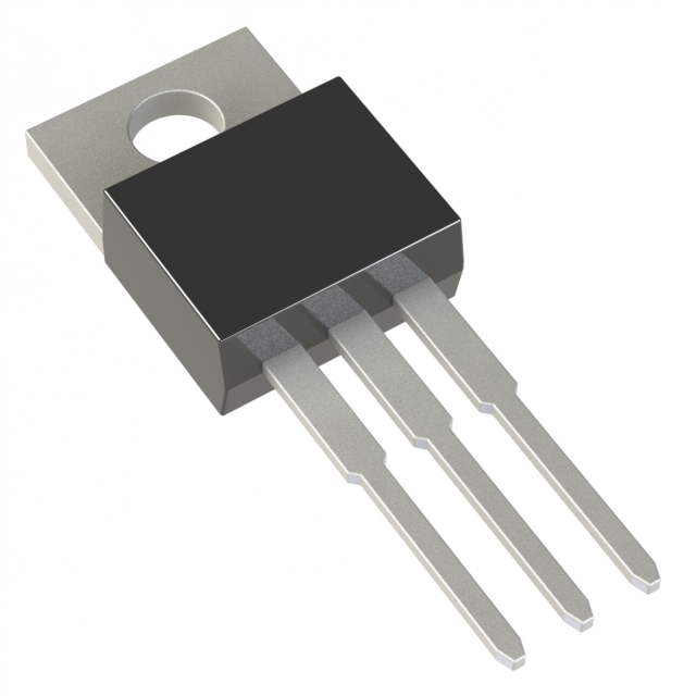
The FCP125N65S3 is an N-Channel 650V 24A MOSFET manufactured by onsemi in the SuperFET® III series, housed in a TO-220-3 through-hole package. This device is classified as "Not For New Designs," indicating it has reached end-of-life status in onsemi's product portfolio. The 650V drain-to-source voltage rating and 24A continuous drain current make it suitable for high-voltage switching applications requiring moderate current handling.
Due to its discontinued design status, equivalent and substitute parts from active product lines are necessary for ongoing production, maintenance, and new system implementations. Substitute devices must maintain compatibility across critical electrical parameters including voltage rating, current capacity, gate charge characteristics, and thermal performance while accommodating the TO-220-3 package standard.
Substiute Parts
Key Parameters
| Parameter | FCP125N65S3 | Unit |
|---|---|---|
| Drain to Source Voltage (Vdss) | 650 | V |
| Continuous Drain Current (Id) @ 25°C | 24 | A |
| Rds On (Max) @ 12A, 10V | 125 | mOhm |
| Gate Charge (Qg) @ 10V | 46 | nC |
| Vgs(th) (Max) @ 2.4mA | 4.5 | V |
| Input Capacitance (Ciss) @ 400V | 1940 | pF |
| Power Dissipation (Max) | 181 | W |
| Operating Temperature Range | -55 to 150 | °C |
| Package Type | TO-220-3 | — |
| Mounting Type | Through Hole | — |
Substitute Part Grouping Explanation
Substitution of the FCP125N65S3 is determined by the following critical electrical and mechanical parameters:
Voltage Rating Compatibility: Substitute devices must maintain a Vdss rating equal to or greater than 650V to ensure safe operation in the original application circuit. Devices rated at 600V represent a lower voltage class and introduce risk in high-voltage transient conditions.
Current Capacity: The continuous drain current (Id) of substitute parts must equal or exceed 24A at 25°C to handle the same load conditions without thermal stress.
On-State Resistance (Rds On): This parameter directly affects power dissipation and thermal performance. Substitute devices with lower Rds On values improve efficiency; higher values increase heat generation and may require thermal management adjustments.
Gate Charge (Qg): Gate charge influences switching speed and driver circuit requirements. Substitute parts with similar gate charge characteristics maintain compatible gate drive circuit performance.
Package and Mounting: All substitute parts must use the TO-220-3 through-hole package to ensure mechanical and electrical compatibility with existing PCB layouts and thermal management solutions.
Operating Temperature Range: Substitute devices must support the full -55°C to 150°C operating range to maintain reliability across all environmental conditions.
Product Status and Compliance: Active product status and RoHS3 compliance are preferred to ensure long-term availability and regulatory conformance.
Parameter Comparison
| Parameter | FCP125N65S3 | AOT42S60L | IPP60R099C7XKSA1 | IXFP34N65X2 | IXKP35N60C5 | STP34NM60ND | Unit |
|---|---|---|---|---|---|---|---|
| Vdss | 650 | 600 | 600 | 650 | 600 | 600 | V |
| Id @ 25°C | 24 | 37 | 22 | 34 | 35 | 29 | A |
| Rds On (Max) @ 10V | 125 | 99 | 99 | 105 | 100 | 110 | mOhm |
| Gate Charge (Qg) @ 10V | 46 | 40 | 42 | 56 | 70 | 80.4 | nC |
| Vgs(th) (Max) | 4.5 | 3.8 | 4.0 | 5.5 | 3.9 | 5.0 | V |
| Input Capacitance (Ciss) | 1940 | 2154 | 1819 | 3330 | 2800 | 2785 | pF |
| Power Dissipation (Max) | 181 | 417 | 110 | 540 | — | 190 | W |
| Operating Temperature | -55 to 150 | -55 to 150 | -55 to 150 | -55 to 150 | -40 to 150 | — | °C |
| Package | TO-220-3 | TO-220-3 | TO-220-3 | TO-220-3 | TO-220-3 | TO-220-3 | — |
| Product Status | Not For New Designs | Not For New Designs | Active | Active | Active | Active | — |
| RoHS3 Compliance | Yes | Yes | Yes | Yes | Yes | Yes | — |
Engineering Selection Recommendations
Primary Substitute: IXFP34N65X2
The IXFP34N65X2 from IXYS is the most direct substitute for the FCP125N65S3. Both devices share the same 650V Vdss rating, maintaining voltage class compatibility. The IXFP34N65X2 provides 34A continuous drain current, exceeding the 24A requirement with a 42% current margin. The on-state resistance of 105 mOhm is lower than the original 125 mOhm, resulting in improved efficiency and reduced thermal dissipation. Gate charge of 56 nC is slightly elevated compared to 46 nC, requiring minimal adjustment to gate drive circuits. The device operates across the full -55°C to 150°C temperature range and maintains active product status with RoHS3 compliance, ensuring long-term availability and regulatory conformance.
Secondary Substitute: IPP60R099C7XKSA1
The IPP60R099C7XKSA1 from Infineon Technologies (CoolMOS™ C7 series) operates at 600V, representing a lower voltage class than the original 650V device. This substitution is suitable only for applications where transient overvoltage protection is confirmed to remain below 600V. The device delivers 22A continuous current, slightly below the 24A specification, and features a 99 mOhm on-state resistance with improved efficiency. Gate charge of 42 nC is lower than the original, reducing switching losses. The device maintains active product status and full RoHS3 compliance. Operating temperature range is -55°C to 150°C.
Tertiary Substitute: STP34NM60ND
The STP34NM60ND from STMicroelectronics (FDmesh™ II series) operates at 600V and delivers 29A continuous current, exceeding the 24A requirement. On-state resistance of 110 mOhm is comparable to the original specification. Gate charge of 80.4 nC is significantly elevated, requiring gate drive circuit verification to ensure adequate switching speed. The device maintains active product status and RoHS3 compliance. Operating temperature range extends to 150°C maximum. This device is suitable for applications where gate charge elevation does not compromise system performance.
Alternative Substitute: AOT42S60L
The AOT42S60L from Alpha & Omega Semiconductor Inc. (aMOS™ series) operates at 600V with 37A continuous current capacity. On-state resistance of 99 mOhm provides improved efficiency. Gate charge of 40 nC is lower than the original, reducing switching losses. However, this device carries "Not For New Designs" status, limiting its suitability for new implementations. It remains available for legacy system maintenance and repair applications.
Voltage Rating Consideration:
Devices rated at 600V (AOT42S60L, IPP60R099C7XKSA1, IXKP35N60C5, STP34NM60ND) represent a lower voltage class than the original 650V specification. Substitution with 600V devices is permissible only when circuit design analysis confirms that maximum transient overvoltage conditions remain below 600V. Applications with uncontrolled voltage transients or snubber-free switching require the 650V-rated IXFP34N65X2.
Frequently Asked Questions (FAQ)
Q: Can I use a 600V-rated MOSFET to replace the 650V FCP125N65S3?
A: Substitution with 600V devices is permissible only when circuit analysis confirms that all transient overvoltage conditions remain below 600V. The original 650V rating provides a 50V safety margin above nominal operating voltage. Applications with uncontrolled switching transients, inductive load switching, or absence of snubber circuits require the 650V-rated IXFP34N65X2 to maintain design margin.
Q: What is the impact of higher gate charge on my gate drive circuit?
A: Gate charge (Qg) determines the total charge that must be supplied to the gate to achieve full on-state conduction. Devices with higher gate charge (such as STP34NM60ND at 80.4 nC versus the original 46 nC) require longer gate charging time or higher gate drive current. Verify that your gate driver IC can supply sufficient current at the required switching frequency. Lower gate charge devices (IPP60R099C7XKSA1 at 42 nC) reduce gate drive power dissipation and allow higher switching frequencies.
Q: Are all substitute parts compatible with my existing PCB layout?
A: All listed substitute parts use the TO-220-3 through-hole package, ensuring mechanical and electrical compatibility with existing PCB layouts. Pin assignments are identical: Gate (pin 1), Drain (pin 2), Source (pin 3). Thermal management characteristics may differ due to variations in on-state resistance and power dissipation; verify that existing heatsinks provide adequate thermal performance for the selected substitute device.
Q: Which substitute part offers the best efficiency improvement?
A: The AOT42S60L and IPP60R099C7XKSA1 both feature 99 mOhm on-state resistance, compared to 125 mOhm for the original FCP125N65S3, representing a 21% reduction in conduction losses. The IXFP34N65X2 provides 105 mOhm resistance with a 16% improvement. Lower on-state resistance reduces thermal dissipation and improves overall system efficiency. However, voltage rating and current capacity requirements must be satisfied first.
Q: What is the difference between "Active" and "Not For New Designs" product status?
A: "Active" status indicates the manufacturer continues production and supports the device for new designs. "Not For New Designs" status indicates the device has reached end-of-life and is available only for legacy system maintenance and repair. For new implementations, select devices with "Active" status: IXFP34N65X2, IPP60R099C7XKSA1, IXKP35N60C5, or STP34NM60ND.
Q: How do I verify that a substitute part will work in my application?
A: Confirm that the substitute device meets or exceeds the following minimum requirements: (1) Vdss rating equal to or greater than 650V, or 600V with verified transient overvoltage analysis; (2) Continuous drain current (Id) equal to or greater than 24A; (3) Operating temperature range includes -55°C to 150°C; (4) TO-220-3 package for PCB compatibility; (5) Gate charge compatible with your gate drive circuit. Perform thermal analysis to confirm that on-state resistance and power dissipation remain within acceptable limits for your heatsink design.
Q: Why do some substitute parts have higher gate charge?
A: Gate charge is determined by the internal capacitance of the MOSFET die and the gate oxide thickness. Devices optimized for lower on-state resistance often exhibit higher gate charge due to larger die area. Conversely, devices optimized for fast switching may have lower gate charge but higher on-state resistance. Select the substitute part that best balances your application's requirements for switching speed, conduction losses, and gate drive capability.
Alternative Parts

SJ6012L2TP
Littelfuse Inc.
6 Alternative Parts

JMK107BBJ476MA-RE
Taiyo Yuden
10 Alternative Parts

GMK107BBJ475MA-T
Taiyo Yuden
5 Alternative Parts
SJ6020N2ARP
Littelfuse Inc.
3 Alternative Parts
SJ6025R2ATP
Littelfuse Inc.
4 Alternative Parts

2474-05L
API Delevan Inc.
1 Alternative Parts

4590R-684K
API Delevan Inc.
1 Alternative Parts

CM6560R-334
API Delevan Inc.
1 Alternative Parts

CM6460-104
API Delevan Inc.
1 Alternative Parts

5526-12
API Delevan Inc.
1 Alternative Parts