


Request Quote
(Ships tomorrow)
DM365ZCES Equivalent & Substitute Parts
Part Overview
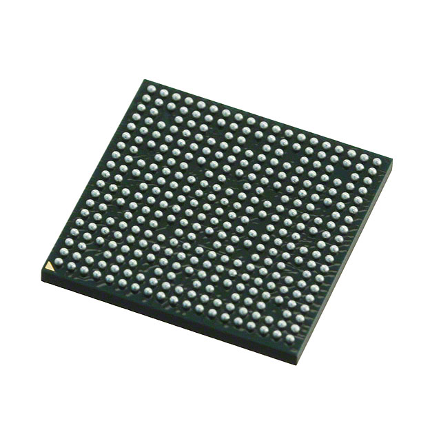
The DM365ZCES is a Digital Media System-on-Chip (DMSoC) from Texas Instruments' TMS320DM3x DaVinci™ series, designed for embedded video and imaging applications. This component integrates a 300MHz processor with comprehensive multimedia interfaces including Ethernet, USB, SPI, I2C, and McBSP connectivity. The device is currently in Last Time Buy status, indicating end-of-life production. Identifying equivalent substitute parts is essential for design continuity, long-term supply chain planning, and new product development where active alternatives are required.
Substiute Parts
Key Parameters
| Parameter | Value |
|---|---|
| Manufacturer Part Number | DM365ZCES |
| Manufacturer | Texas Instruments |
| Series | TMS320DM3x, DaVinci™ |
| Type | Digital Media System-on-Chip (DMSoC) |
| Clock Rate | 300MHz |
| Package / Case | 338-LFBGA (13x13) |
| Voltage - Core | 1.20V |
| Voltage - I/O | 1.8V, 3.3V |
| On-Chip RAM | 56kB |
| Non-Volatile Memory | ROM (16kB) |
| Operating Temperature | 0°C ~ 85°C (TC) |
| RoHS Status | ROHS3 Compliant |
| Product Status | Last Time Buy |
Substitute Part Grouping Explanation
Substitution eligibility for the DM365ZCES is determined by the following critical parameters:
Package Compatibility: Both the main part and substitute must use the 338-LFBGA (13x13) package to ensure PCB footprint and mechanical compatibility without redesign.
Voltage Specifications: Core voltage (1.20V) and I/O voltage levels (1.8V, 3.3V) must match to maintain power delivery architecture and signal integrity.
Memory Configuration: On-chip RAM (56kB) and ROM (16kB) must be identical to preserve firmware and runtime memory requirements.
Interface Support: All required interfaces (EBI/EMI, Ethernet, I2C, McBSP, SPI, UART, USB) must be present in the substitute part.
Operating Temperature Range: The 0°C ~ 85°C (TC) specification must be maintained for thermal design compliance.
Compliance Standards: RoHS3 compliance, MSL rating (3, 168 Hours), and REACH status must be equivalent or superior.
The TMS320DM365ZCE21 meets all these criteria, with the primary difference being a reduced clock rate (216MHz versus 300MHz), which represents a functional downgrade but maintains full architectural compatibility.
Parameter Comparison
| Parameter | DM365ZCES (Main Part) | TMS320DM365ZCE21 (Substitute) | Compatibility |
|---|---|---|---|
| Manufacturer | Texas Instruments | Texas Instruments | Identical |
| Series | TMS320DM3x, DaVinci™ | TMS320DM3x, DaVinci™ | Identical |
| Type | Digital Media System-on-Chip (DMSoC) | Digital Media System-on-Chip (DMSoC) | Identical |
| Clock Rate | 300MHz | 216MHz | Reduced Performance |
| Package / Case | 338-LFBGA (13x13) | 338-LFBGA (13x13) | Identical |
| Voltage - Core | 1.20V | 1.20V | Identical |
| Voltage - I/O | 1.8V, 3.3V | 1.8V, 3.3V | Identical |
| On-Chip RAM | 56kB | 56kB | Identical |
| Non-Volatile Memory | ROM (16kB) | ROM (16kB) | Identical |
| Operating Temperature | 0°C ~ 85°C (TC) | 0°C ~ 85°C (TC) | Identical |
| Interface | EBI/EMI, Ethernet, I2C, McBSP, SPI, UART, USB | EBI/EMI, Ethernet, I2C, McBSP, SPI, UART, USB | Identical |
| RoHS Status | ROHS3 Compliant | ROHS3 Compliant | Identical |
| MSL Rating | 3 (168 Hours) | 3 (168 Hours) | Identical |
| Product Status | Last Time Buy | Active | Substitute is Active |
Engineering Selection Recommendations
For Last Time Buy Mitigation: The DM365ZCES is in Last Time Buy status, making long-term supply unavailable. The TMS320DM365ZCE21 is an active product from the same manufacturer and series, providing supply continuity for new designs and production extensions.
For Existing Designs: Designs currently using the DM365ZCES at full 300MHz performance should evaluate whether the 216MHz clock rate of the TMS320DM365ZCE21 meets application throughput requirements. If performance headroom exists in the original design, the substitute is directly compatible without PCB modifications.
For New Designs: New product development should prioritize the TMS320DM365ZCE21 due to its active product status and guaranteed long-term availability. The identical package, voltage specifications, memory configuration, and interface set ensure seamless integration into existing reference designs.
Compliance Verification: Both parts maintain ROHS3 compliance, identical MSL ratings, and equivalent REACH status, satisfying regulatory and supply chain requirements without additional qualification.
Frequently Asked Questions (FAQ)
Q: Can the TMS320DM365ZCE21 be used as a direct drop-in replacement for the DM365ZCES?
A: Yes, for applications where the 216MHz clock rate is sufficient. The identical 338-LFBGA package, voltage specifications, memory configuration, and interface set enable direct PCB compatibility without layout modifications. Performance-critical applications must validate that reduced clock speed does not impact system throughput.
Q: What is the primary difference between these two parts?
A: The clock rate differs: DM365ZCES operates at 300MHz, while TMS320DM365ZCE21 operates at 216MHz. All other electrical and mechanical parameters are identical.
Q: Why is the DM365ZCES in Last Time Buy status?
A: Last Time Buy status indicates Texas Instruments has discontinued production and is accepting final orders before end-of-life. The TMS320DM365ZCE21 remains in active production as the current product offering in this performance tier.
Q: Are there any PCB layout changes required when switching from DM365ZCES to TMS320DM365ZCE21?
A: No. Both parts use the identical 338-LFBGA (13x13) package, eliminating the need for PCB redesign or re-layout.
Q: Do both parts support the same interfaces?
A: Yes. Both the DM365ZCES and TMS320DM365ZCE21 support EBI/EMI, Ethernet, I2C, McBSP, SPI, UART, and USB interfaces identically.
Q: What are the compliance and certification implications of this substitution?
A: Both parts are ROHS3 compliant, carry identical MSL ratings (3, 168 Hours), and maintain equivalent REACH status. No additional compliance qualification is required for the substitution.
Q: Is the TMS320DM365ZCE21 suitable for high-performance video processing applications?
A: The 216MHz clock rate of the TMS320DM365ZCE21 is lower than the original 300MHz specification. Applications requiring maximum video throughput should evaluate whether this reduced performance meets real-time processing requirements before selection.
Alternative Parts

SJ6012L2TP
Littelfuse Inc.
6 Alternative Parts

JMK107BBJ476MA-RE
Taiyo Yuden
10 Alternative Parts

GMK107BBJ475MA-T
Taiyo Yuden
5 Alternative Parts
SJ6020N2ARP
Littelfuse Inc.
3 Alternative Parts
SJ6025R2ATP
Littelfuse Inc.
4 Alternative Parts

2474-05L
API Delevan Inc.
1 Alternative Parts

4590R-684K
API Delevan Inc.
1 Alternative Parts

CM6560R-334
API Delevan Inc.
1 Alternative Parts

CM6460-104
API Delevan Inc.
1 Alternative Parts

5526-12
API Delevan Inc.
1 Alternative Parts