


Request Quote
(Ships tomorrow)
DG2011DXA-T1-E3 Equivalent & Substitute Parts
Part Overview
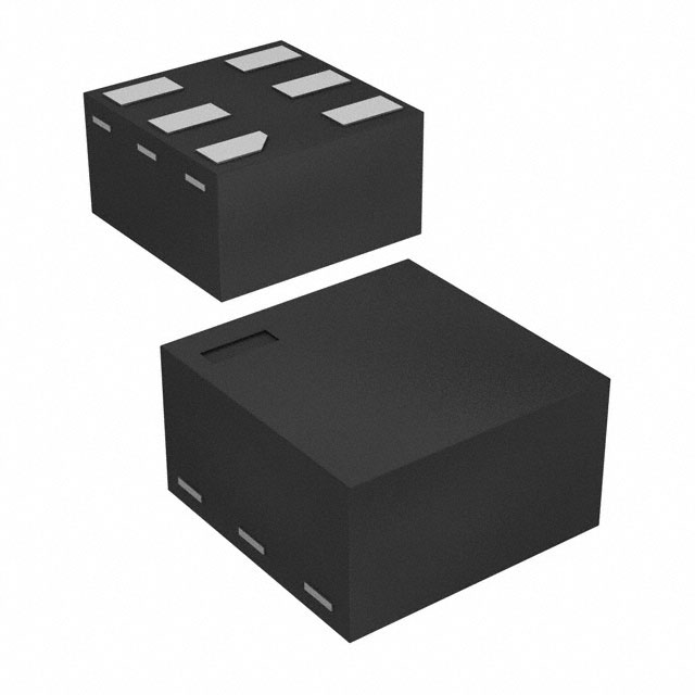
The DG2011DXA-T1-E3 is a single-circuit SPDT (Single Pole Double Throw) analog switch manufactured by Vishay Siliconix, designed for signal routing and multiplexing applications in low-voltage systems. The device operates across a supply voltage range of 1.8V to 5.5V and is packaged in SC-89-6 (SOT-666) surface mount configuration.
This part is classified as obsolete. Identifying equivalent and substitute components is necessary to ensure design continuity, maintain supply chain reliability, and support long-term product availability for applications currently utilizing this switch.
Substiute Parts
Key Parameters
| Parameter | Value |
|---|---|
| Switch Circuit Type | SPDT (2:1 Multiplexer) |
| Number of Circuits | 1 |
| On-State Resistance (Max) | 2.7Ω |
| Channel-to-Channel Matching (ΔRon Max) | 200mΩ |
| Supply Voltage Range (Single) | 1.8V ~ 5.5V |
| Switch Time (Ton/Toff Max) | 75ns / 59ns |
| Charge Injection | 2pC |
| Channel Capacitance (Off-State) | 29pF |
| Leakage Current (Max) | 1nA |
| Operating Temperature | -40°C ~ 85°C |
| Package Type | SOT-563, SOT-666 |
| RoHS Status | ROHS3 Compliant |
| MSL Rating | 1 (Unlimited) |
Substitute Part Grouping Explanation
Substitution of the DG2011DXA-T1-E3 is determined by the following core electrical and mechanical parameters:
- Switch topology: SPDT configuration with 2:1 multiplexing capability
- Single-circuit requirement: One independent switch circuit
- Supply voltage compatibility: Operating range must encompass or be compatible with 1.8V ~ 5.5V
- On-state resistance: Maximum allowable resistance for signal integrity in the application
- Switching speed: Ton and Toff specifications for timing-critical applications
- Package compatibility: Surface mount form factor suitable for existing PCB layouts
- Compliance standards: RoHS3 compliance and MSL rating for manufacturing and environmental requirements
The DG4157EDN-T1-GE4 qualifies as a substitute based on matching these core parameters while offering improved electrical performance characteristics.
Parameter Comparison
| Parameter | DG2011DXA-T1-E3 | DG4157EDN-T1-GE4 |
|---|---|---|
| Manufacturer | Vishay Siliconix | Vishay Siliconix |
| Switch Circuit | SPDT | SPDT |
| Multiplexer Configuration | 2:1 | 2:1 |
| Number of Circuits | 1 | 1 |
| On-State Resistance (Max) | 2.7Ω | 1.2Ω |
| Channel-to-Channel Matching (ΔRon Max) | 200mΩ | 120mΩ |
| Supply Voltage Range (Single) | 1.8V ~ 5.5V | 1.65V ~ 5.5V |
| Switch Time Ton (Max) | 75ns | 32ns |
| Switch Time Toff (Max) | 59ns | 28ns |
| Charge Injection | 2pC | -5pC |
| Leakage Current (Max) | 1nA | 3nA |
| Operating Temperature | -40°C ~ 85°C | -40°C ~ 85°C |
| Mounting Type | Surface Mount | Surface Mount |
| Package / Case | SOT-563, SOT-666 | 6-XFDFN |
| RoHS Status | ROHS3 Compliant | ROHS3 Compliant |
| MSL Rating | 1 (Unlimited) | 1 (Unlimited) |
Engineering Selection Recommendations
The DG4157EDN-T1-GE4 is the manufacturer-recommended substitute for the obsolete DG2011DXA-T1-E3. Both devices are manufactured by Vishay Siliconix and maintain ROHS3 compliance and MSL Level 1 ratings, ensuring compatibility with current manufacturing and environmental standards.
The DG4157EDN-T1-GE4 offers superior electrical performance with lower on-state resistance (1.2Ω vs. 2.7Ω), faster switching times (32ns/28ns vs. 75ns/59ns), and improved channel matching (120mΩ vs. 200mΩ). The supply voltage range of 1.65V ~ 5.5V is compatible with applications designed for the original part's 1.8V ~ 5.5V specification.
The primary design consideration is package transition from SC-89-6 (SOT-666) to 6-µDFN (1x1). PCB layout modifications are required to accommodate the different footprint geometry.
Frequently Asked Questions (FAQ)
Q: Can the DG4157EDN-T1-GE4 directly replace the DG2011DXA-T1-E3 without circuit modifications?
A: Electrical substitution is valid. The DG4157EDN-T1-GE4 maintains SPDT 2:1 multiplexer functionality with compatible supply voltage range and operating temperature. However, the package change from SOT-666 to 6-µDFN requires PCB footprint redesign and layout modifications.
Q: What are the key electrical differences between these parts?
A: The DG4157EDN-T1-GE4 provides lower on-state resistance (1.2Ω vs. 2.7Ω), faster switching performance (32ns/28ns vs. 75ns/59ns), and tighter channel matching (120mΩ vs. 200mΩ). These improvements enhance signal integrity and reduce switching delays in multiplexing applications.
Q: Are both parts compliant with current manufacturing standards?
A: Yes. Both the DG2011DXA-T1-E3 and DG4157EDN-T1-GE4 are ROHS3 compliant with MSL Level 1 ratings, meeting current environmental and manufacturing requirements.
Q: What is the primary limitation when substituting these parts?
A: Package incompatibility is the primary design constraint. The original SC-89-6 (SOT-666) footprint differs from the 6-µDFN (1x1) package of the substitute. PCB redesign is necessary to accommodate the new package geometry and pin configuration.
Q: Is the supply voltage range compatible for all applications?
A: The DG4157EDN-T1-GE4 operates at 1.65V minimum versus 1.8V for the original part. Applications operating at 1.65V ~ 1.8V will function with the substitute but not with the original. Applications above 1.8V are compatible with both devices.
Alternative Parts

SJ6012L2TP
Littelfuse Inc.
6 Alternative Parts

JMK107BBJ476MA-RE
Taiyo Yuden
10 Alternative Parts

GMK107BBJ475MA-T
Taiyo Yuden
5 Alternative Parts
SJ6020N2ARP
Littelfuse Inc.
3 Alternative Parts
SJ6025R2ATP
Littelfuse Inc.
4 Alternative Parts

2474-05L
API Delevan Inc.
1 Alternative Parts

4590R-684K
API Delevan Inc.
1 Alternative Parts

CM6560R-334
API Delevan Inc.
1 Alternative Parts

CM6460-104
API Delevan Inc.
1 Alternative Parts

5526-12
API Delevan Inc.
1 Alternative Parts