


Request Quote
(Ships tomorrow)
CPH6445-TL-W N-Channel MOSFET Equivalent & Substitute Parts
Part Overview
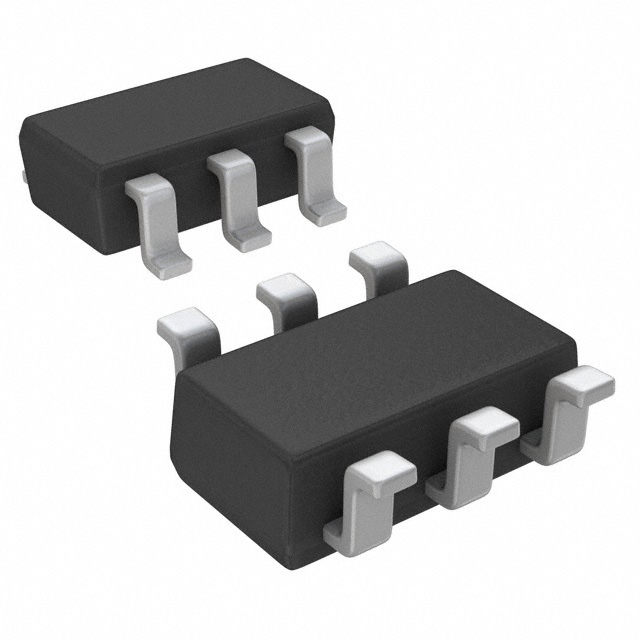
The CPH6445-TL-W is an N-Channel MOSFET manufactured by onsemi, rated for 60V drain-to-source voltage with a continuous drain current of 3.5A at 25°C. This device is packaged in a 6-CPH (SOT-23-6) surface mount configuration and is designed for general-purpose switching applications requiring moderate current handling and low on-resistance characteristics.
The CPH6445-TL-W has reached obsolete product status. Identifying equivalent and substitute parts is necessary to maintain design continuity, ensure supply chain availability, and support ongoing production requirements for applications currently utilizing this component.
Substiute Parts
Key Parameters
| Parameter | Value | Unit |
|---|---|---|
| FET Type | N-Channel | — |
| Drain to Source Voltage (Vdss) | 60 | V |
| Continuous Drain Current (Id) @ 25°C | 3.5 | A |
| On-Resistance (Rds On Max) @ Id, Vgs | 117 mOhm @ 1.5A, 10V | — |
| Gate Charge (Qg Max) @ Vgs | 6.8 | nC @ 10V |
| Input Capacitance (Ciss Max) @ Vds | 310 | pF @ 20V |
| Power Dissipation (Max) | 1.6 | W |
| Operating Temperature (TJ) | 150 | °C |
| Package Type | SOT-23-6 | — |
| Mounting Type | Surface Mount | — |
| RoHS Status | ROHS3 Compliant | — |
| Moisture Sensitivity Level (MSL) | 1 (Unlimited) | — |
Substitute Part Grouping Explanation
Substitute parts for the CPH6445-TL-W are identified based on strict electrical and mechanical parameter compatibility within the N-Channel MOSFET category. The substitution criteria are:
Electrical Compatibility Requirements:
- FET Type: N-Channel (identical)
- Drain to Source Voltage (Vdss): 60V (identical or higher)
- Continuous Drain Current (Id): Equal to or greater than 3.5A
- Power Dissipation: 1.6W or greater
- Gate-to-Source Voltage (Vgs Max): ±20V (identical)
- Operating Temperature Range: Minimum 150°C junction temperature
Mechanical Compatibility Requirements:
- Package Type: SOT-23-6 or equivalent surface mount 6-pin configuration
- Mounting Type: Surface Mount
- RoHS Compliance: ROHS3 Compliant
- Moisture Sensitivity Level: MSL 1 or better
The FDC5661N-F085 meets all substitution criteria and is classified as an active product with enhanced electrical performance characteristics.
Parameter Comparison
| Parameter | CPH6445-TL-W | FDC5661N-F085 | Unit |
|---|---|---|---|
| Manufacturer | onsemi | onsemi | — |
| FET Type | N-Channel | N-Channel | — |
| Drain to Source Voltage (Vdss) | 60 | 60 | V |
| Continuous Drain Current (Id) @ 25°C | 3.5 | 4.3 | A |
| On-Resistance (Rds On Max) @ Vgs 10V | 117 mOhm @ 1.5A | 47 mOhm @ 4.3A | — |
| Gate Charge (Qg Max) @ Vgs 10V | 6.8 | 19 | nC |
| Input Capacitance (Ciss Max) | 310 pF @ 20V | 763 pF @ 25V | — |
| Power Dissipation (Max) | 1.6 | 1.6 | W |
| Operating Temperature (TJ) | 150 | −55 to 150 | °C |
| Package Type | SOT-23-6 | SOT-23-6 Thin, TSOT-23-6 | — |
| Mounting Type | Surface Mount | Surface Mount | — |
| RoHS Status | ROHS3 Compliant | ROHS3 Compliant | — |
| Moisture Sensitivity Level (MSL) | 1 (Unlimited) | 1 (Unlimited) | — |
| Product Status | Obsolete | Active | — |
Engineering Selection Recommendations
The FDC5661N-F085 is the qualified substitute for the obsolete CPH6445-TL-W. Both devices are manufactured by onsemi and share identical voltage ratings, power dissipation limits, and package configurations.
Substitution Basis:
The FDC5661N-F085 exceeds the electrical requirements of the CPH6445-TL-W across all critical parameters. The substitute device provides higher continuous drain current (4.3A versus 3.5A), lower on-resistance (47 mOhm versus 117 mOhm at rated conditions), and an extended operating temperature range (−55°C to 150°C versus 150°C maximum). Both devices maintain identical power dissipation ratings and comply with ROHS3 and REACH requirements.
The FDC5661N-F085 carries active product status and includes AEC-Q101 automotive qualification, indicating ongoing manufacturer support and supply chain availability. The device is available in standard SOT-23-6 and TSOT-23-6 package variants, both compatible with existing PCB layouts designed for the CPH6445-TL-W.
Compliance certifications (ROHS3, REACH, EAR99 ECCN classification) are identical between the main part and substitute, ensuring regulatory continuity in applications subject to environmental and export control requirements.
Frequently Asked Questions (FAQ)
Q: Can the FDC5661N-F085 directly replace the CPH6445-TL-W in existing designs?
A: Yes. Both devices share identical Vdss (60V), power dissipation (1.6W), package type (SOT-23-6), and pin configuration. The FDC5661N-F085 provides equal or superior electrical performance and is pin-compatible for direct substitution.
Q: What are the key electrical differences between these devices?
A: The FDC5661N-F085 provides higher continuous drain current (4.3A versus 3.5A) and significantly lower on-resistance (47 mOhm versus 117 mOhm at 10V gate voltage). Gate charge is higher (19 nC versus 6.8 nC), and input capacitance is increased (763 pF versus 310 pF). These differences result in improved current handling and reduced conduction losses in the substitute device.
Q: Are there package compatibility concerns?
A: No. Both devices use SOT-23-6 surface mount packaging. The FDC5661N-F085 is available in standard SOT-23-6 and TSOT-23-6 (thin variant) configurations. Existing PCB designs and reflow profiles for the CPH6445-TL-W are compatible with the FDC5661N-F085.
Q: What is the product status difference, and why does it matter?
A: The CPH6445-TL-W is obsolete, indicating discontinued manufacturing and limited supply availability. The FDC5661N-F085 is active, ensuring ongoing production, documented supply chain availability, and manufacturer technical support. Active status is critical for long-term design support and production continuity.
Q: Are compliance and certification requirements met by the substitute?
A: Yes. The FDC5661N-F085 is ROHS3 compliant, REACH unaffected, and carries EAR99 ECCN classification, identical to the CPH6445-TL-W. The substitute additionally qualifies for AEC-Q101 automotive applications, providing broader qualification coverage.
Q: What is the operating temperature range difference?
A: The CPH6445-TL-W specifies a maximum junction temperature of 150°C. The FDC5661N-F085 operates across −55°C to 150°C, providing extended low-temperature performance. Applications operating within the CPH6445-TL-W temperature envelope are fully supported by the substitute.
Q: Is the higher gate charge of the FDC5661N-F085 a concern?
A: Gate charge (19 nC versus 6.8 nC) affects gate drive circuit design and switching speed. Applications with gate drive circuits designed for the CPH6445-TL-W may experience slightly slower switching transitions with the FDC5661N-F085. Verify gate drive capability for high-frequency switching applications above 1 MHz.
Alternative Parts

SJ6012L2TP
Littelfuse Inc.
6 Alternative Parts

JMK107BBJ476MA-RE
Taiyo Yuden
10 Alternative Parts

GMK107BBJ475MA-T
Taiyo Yuden
5 Alternative Parts
SJ6020N2ARP
Littelfuse Inc.
3 Alternative Parts
SJ6025R2ATP
Littelfuse Inc.
4 Alternative Parts

2474-05L
API Delevan Inc.
1 Alternative Parts

4590R-684K
API Delevan Inc.
1 Alternative Parts

CM6560R-334
API Delevan Inc.
1 Alternative Parts

CM6460-104
API Delevan Inc.
1 Alternative Parts

5526-12
API Delevan Inc.
1 Alternative Parts