


Request Quote
(Ships tomorrow)
CP210-2N4416A-CT20 Equivalent & Substitute Parts
Part Overview
The CP210-2N4416A-CT20 is an N-Channel JFET (Junction Field-Effect Transistor) manufactured by Central Semiconductor Corp, designed for surface mount die applications. This component operates at 35 V breakdown voltage with a maximum drain current of 15 mA and is rated for temperatures from -65°C to 150°C. The part is currently classified as obsolete, making identification of suitable substitute components essential for ongoing design support and production continuity.
Substiute Parts
Key Parameters
| Parameter | Value | Unit |
|---|---|---|
| FET Type | N-Channel | — |
| Voltage - Breakdown (V(BR)GSS) | 35 | V |
| Drain to Source Voltage (Vdss) | 35 | V |
| Current - Drain (Idss) @ Vds (Vgs=0) | 5 mA @ 20 V | mA |
| Current Drain (Id) - Max | 15 | mA |
| Voltage - Cutoff (VGS off) @ Id | 2.5 V @ 1 nA | V |
| Input Capacitance (Ciss) (Max) @ Vds | 4 pF @ 15 V | pF |
| Operating Temperature Range | -65 to 150 | °C |
| Mounting Type | Surface Mount | — |
| Package / Case | Die | — |
Substitute Part Grouping Explanation
Substitution of the CP210-2N4416A-CT20 is determined by the following critical electrical and mechanical parameters:
Electrical Compatibility Criteria:
- FET Type: N-Channel configuration
- Voltage Rating: Minimum 35 V Vdss and V(BR)GSS
- Cutoff Voltage (VGS off): 2.5 V @ 1 nA
- Input Capacitance: Maximum 4.5 pF @ 15 V
Mechanical Compatibility Criteria:
- Mounting Type: Surface Mount
- Operating Temperature Range: -65°C to 150°C minimum
The CP232V-2N4416A-CT20 qualifies as a direct substitute based on matching electrical specifications across all critical parameters. While the maximum drain current differs (5 mA vs. 15 mA), this represents a derating condition acceptable for applications where the original 15 mA specification was not fully utilized. The transition from die packaging to SOT-23 packaging provides improved handling and integration characteristics while maintaining electrical equivalence.
Parameter Comparison
| Parameter | CP210-2N4416A-CT20 (Main) | CP232V-2N4416A-CT20 (Substitute) |
|---|---|---|
| Manufacturer | Central Semiconductor Corp | Central Semiconductor Corp |
| FET Type | N-Channel | N-Channel |
| Voltage - Breakdown (V(BR)GSS) | 35 V | 35 V |
| Drain to Source Voltage (Vdss) | 35 V | 35 V |
| Current - Drain (Idss) @ Vds (Vgs=0) | 5 mA @ 20 V | 5 mA @ 15 V |
| Current Drain (Id) - Max | 15 mA | 5 mA |
| Voltage - Cutoff (VGS off) @ Id | 2.5 V @ 1 nA | 2.5 V @ 1 nA |
| Input Capacitance (Ciss) (Max) @ Vds | 4 pF @ 15 V | 4.5 pF @ 15 V |
| Operating Temperature Range | -65°C to 150°C | -65°C to 150°C |
| Mounting Type | Surface Mount | Surface Mount |
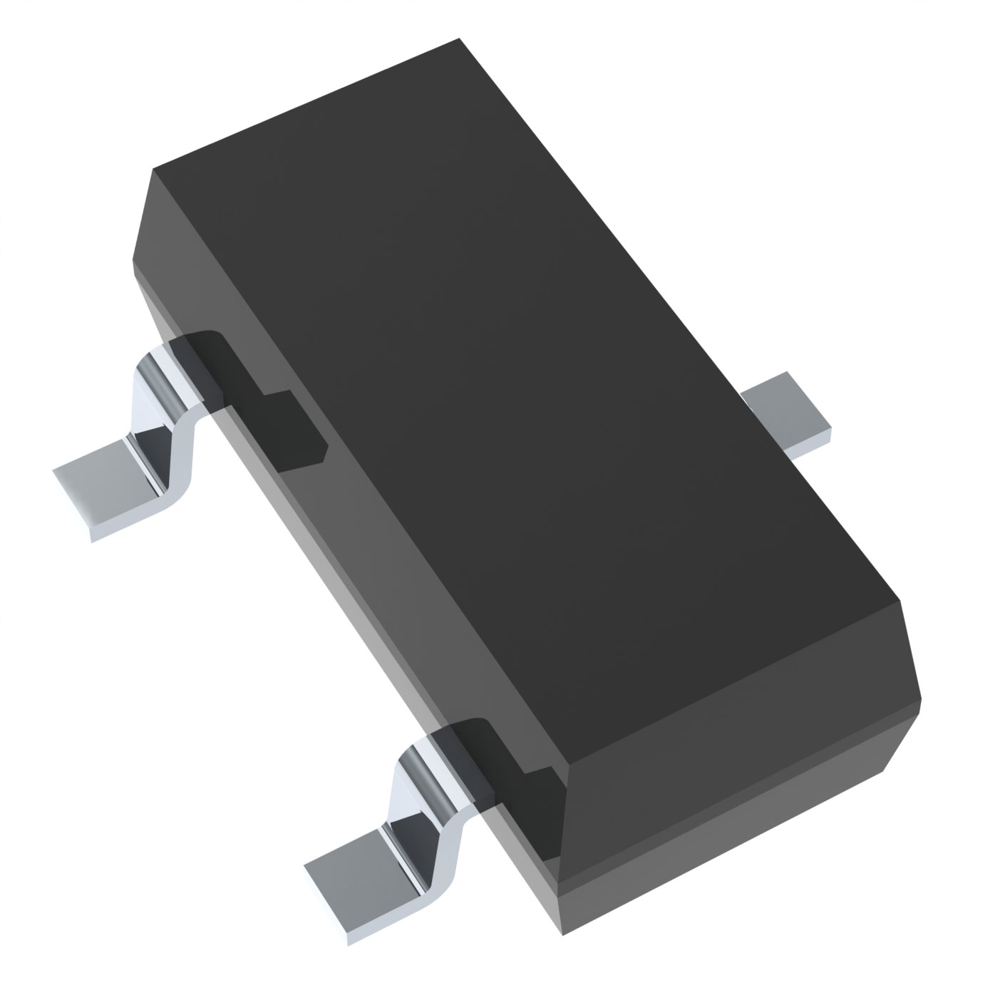
| Package / Case | Die | SOT-23-3 |
| Product Status | Obsolete | Active |
Engineering Selection Recommendations
The CP232V-2N4416A-CT20 is the appropriate substitute for the obsolete CP210-2N4416A-CT20. Selection is based on the following factors:
Product Status: The substitute part maintains active production status with Central Semiconductor Corp, ensuring long-term availability and supply chain continuity.
Electrical Equivalence: All critical electrical parameters match or exceed the original specification. The maximum drain current rating of 5 mA represents a conservative derating from the original 15 mA specification; applications operating within 5 mA maximum drain current will experience no functional degradation.
Compliance & Certifications: The substitute part carries REACH Unaffected status and EAR99 ECCN classification, meeting current regulatory requirements for component procurement and export.
Packaging Transition: Migration from die packaging to SOT-23 surface mount packaging improves component handling, reduces assembly complexity, and provides superior thermal management through the package substrate.
Frequently Asked Questions (FAQ)
Q: Can the CP232V-2N4416A-CT20 directly replace the CP210-2N4416A-CT20 in existing designs?
A: Yes, provided the application does not require drain current exceeding 5 mA. The electrical characteristics, voltage ratings, and temperature range are equivalent. The primary design consideration is the packaging change from die to SOT-23, which may require PCB layout modifications.
Q: What is the significance of the reduced maximum drain current (5 mA vs. 15 mA)?
A: The substitute part is rated for a maximum drain current of 5 mA. If your circuit design operates the original part at currents below 5 mA, the substitute is fully compatible. If the original design requires drain currents between 5 mA and 15 mA, the substitute cannot be used without circuit redesign.
Q: Are there any thermal management differences between the die and SOT-23 packages?
A: The SOT-23 package includes a substrate that provides improved thermal dissipation compared to bare die. The substitute part is rated for 350 mW maximum power dissipation, which is suitable for most low-power JFET applications.
Q: What certifications apply to the substitute part?
A: The CP232V-2N4416A-CT20 carries REACH Unaffected status, indicating compliance with European chemical regulations. The EAR99 ECCN classification applies for export control purposes.
Q: Are there any differences in input capacitance between the two parts?
A: The input capacitance differs slightly: 4 pF (original) versus 4.5 pF (substitute) at 15 V. This 0.5 pF difference is negligible for most applications and does not affect circuit performance in typical JFET switching or amplification circuits.
Alternative Parts

SJ6012L2TP
Littelfuse Inc.
6 Alternative Parts

JMK107BBJ476MA-RE
Taiyo Yuden
10 Alternative Parts

GMK107BBJ475MA-T
Taiyo Yuden
5 Alternative Parts
SJ6020N2ARP
Littelfuse Inc.
3 Alternative Parts
SJ6025R2ATP
Littelfuse Inc.
4 Alternative Parts

2474-05L
API Delevan Inc.
1 Alternative Parts

4590R-684K
API Delevan Inc.
1 Alternative Parts

CM6560R-334
API Delevan Inc.
1 Alternative Parts

CM6460-104
API Delevan Inc.
1 Alternative Parts

5526-12
API Delevan Inc.
1 Alternative Parts