


Request Quote
(Ships tomorrow)
CLC2005IMP8X Equivalent & Substitute Parts
Part Overview
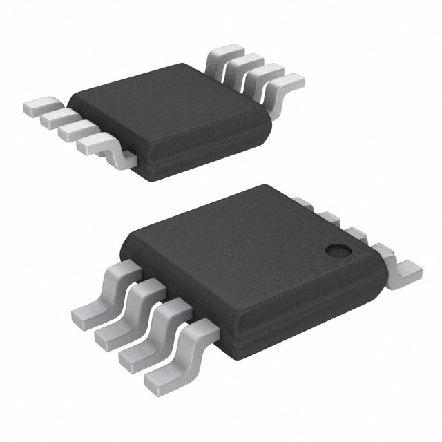
The CLC2005IMP8X is a voltage feedback amplifier integrated circuit manufactured by MaxLinear, Inc., containing two circuits in a rail-to-rail configuration housed in an 8-MSOP package. This device is classified as obsolete, indicating discontinued production and limited availability for new designs. The identification of equivalent substitute parts is necessary to ensure continued component sourcing, maintain design continuity, and support existing inventory management for applications currently utilizing this amplifier.
Substiute Parts
Key Parameters
| Parameter | Value | Unit |
|---|---|---|
| Amplifier Type | Voltage Feedback | — |
| Number of Circuits | 2 | — |
| Output Type | Rail-to-Rail | — |
| Slew Rate | 145 | V/µs |
| Gain Bandwidth Product | 260 | MHz |
| -3dB Bandwidth | 260 | MHz |
| Current - Input Bias | 3 | µA |
| Voltage - Input Offset | 1.6 | mV |
| Current - Supply (x2 Channels) | 4.2 | mA |
| Current - Output / Channel | 55 | mA |
| Voltage - Supply Span (Min) | 2.5 | V |
| Voltage - Supply Span (Max) | 5.5 | V |
| Operating Temperature Range | -40 to 85 | °C |
| Package / Case | 8-TSSOP, 8-MSOP (0.118", 3.00mm Width) | — |
| Mounting Type | Surface Mount | — |
| Moisture Sensitivity Level (MSL) | 1 (Unlimited) | — |
Substitute Part Grouping Explanation
Substitution of the CLC2005IMP8X is determined by strict alignment of electrical and mechanical parameters within the linear amplifier category. The substitute part LT1807IMS8#PBF is grouped as an equivalent based on the following criteria:
Mechanical Compatibility:
- Identical package type: 8-MSOP (0.118", 3.00mm Width)
- Identical mounting type: Surface Mount
- Identical circuit count: 2 circuits per device
- Identical output configuration: Rail-to-Rail
Electrical Parameter Alignment:
- Output type classification: Rail-to-Rail
- Operating temperature range: -40°C to 85°C (identical)
- Minimum supply voltage: 2.5 V (identical)
- Moisture sensitivity level: MSL 1 (Unlimited) (identical)
Functional Category:
- Both devices operate as amplifier integrated circuits in the linear category
- Both support dual-channel configurations
- Both are housed in industry-standard 8-pin MSOP packages suitable for surface mount assembly
Parameter Comparison
| Parameter | CLC2005IMP8X (Main Part) | LT1807IMS8#PBF (Substitute) | Unit |
|---|---|---|---|
| Manufacturer | MaxLinear, Inc. | Analog Devices Inc. | — |
| Product Status | Obsolete | Active | — |
| Amplifier Type | Voltage Feedback | General Purpose | — |
| Number of Circuits | 2 | 2 | — |
| Output Type | Rail-to-Rail | Rail-to-Rail | — |
| Slew Rate | 145 | 140 | V/µs |
| Gain Bandwidth Product | 260 | 325 | MHz |
| -3dB Bandwidth | 260 | — | MHz |
| Current - Input Bias | 3 | 1 | µA |
| Voltage - Input Offset | 1.6 | 0.1 | mV |
| Current - Supply (x2 Channels) | 4.2 | 9 | mA |
| Current - Output / Channel | 55 | 85 | mA |
| Voltage - Supply Span (Min) | 2.5 | 2.5 | V |
| Voltage - Supply Span (Max) | 5.5 | 12.6 | V |
| Operating Temperature Range | -40 to 85 | -40 to 85 | °C |
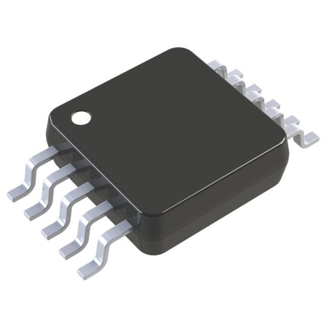
| Package / Case | 8-TSSOP, 8-MSOP (0.118", 3.00mm Width) | 8-TSSOP, 8-MSOP (0.118", 3.00mm Width) | — |
| Mounting Type | Surface Mount | Surface Mount | — |
| Moisture Sensitivity Level (MSL) | 1 (Unlimited) | 1 (Unlimited) | — |
| RoHS Status | — | ROHS3 Compliant | — |
Engineering Selection Recommendations
The LT1807IMS8#PBF from Analog Devices Inc. is identified as the substitute part for the obsolete CLC2005IMP8X based on mechanical and electrical parameter alignment within the 8-MSOP package category.
Product Status Consideration: The CLC2005IMP8X is classified as obsolete with no continued manufacturing. The LT1807IMS8#PBF maintains active product status with current manufacturing and availability, supporting long-term supply chain requirements.
Compliance and Certification: The LT1807IMS8#PBF carries ROHS3 compliance certification, meeting current environmental and regulatory standards. The substitute part is classified under ECCN EAR99, appropriate for general commercial distribution.
Electrical Performance: Both devices operate within the -40°C to 85°C temperature range and share identical minimum supply voltage specifications of 2.5 V. The LT1807IMS8#PBF provides extended maximum supply voltage capability (12.6 V versus 5.5 V), offering broader application flexibility. The substitute part demonstrates improved input offset voltage (0.1 mV versus 1.6 mV) and reduced input bias current (1 µA versus 3 µA), representing enhanced precision characteristics.
Mechanical Compatibility: Both parts utilize identical 8-MSOP surface mount packaging with 0.118" (3.00mm) width, ensuring direct footprint compatibility on existing printed circuit boards without layout modification.
Frequently Asked Questions (FAQ)
Q: Can the LT1807IMS8#PBF directly replace the CLC2005IMP8X in existing designs?
A: The LT1807IMS8#PBF is mechanically compatible with the CLC2005IMP8X, sharing identical 8-MSOP package dimensions and surface mount configuration. Both devices contain two rail-to-rail amplifier circuits. Circuit-level validation is required to confirm electrical performance compatibility within specific application parameters, particularly regarding supply voltage range, slew rate, and bandwidth requirements.
Q: What are the key differences between these two parts?
A: The primary differences are: (1) Product status—CLC2005IMP8X is obsolete; LT1807IMS8#PBF is active; (2) Amplifier classification—voltage feedback versus general purpose; (3) Maximum supply voltage—5.5 V versus 12.6 V; (4) Input offset voltage—1.6 mV versus 0.1 mV; (5) Supply current—4.2 mA versus 9 mA per dual channels; (6) Output current—55 mA versus 85 mA per channel; (7) Gain bandwidth product—260 MHz versus 325 MHz.
Q: Are there any package or pinout differences?
A: Both parts use the 8-MSOP package with identical physical dimensions (0.118" width, 3.00mm). No pinout modifications are required for direct substitution at the board level.
Q: What is the impact of the extended supply voltage range on the LT1807IMS8#PBF?
A: The LT1807IMS8#PBF supports supply voltages up to 12.6 V, compared to 5.5 V maximum for the CLC2005IMP8X. This extended range provides design flexibility for applications requiring higher supply voltages. Designs currently operating within the 2.5 V to 5.5 V range remain fully compatible.
Q: Does the improved input offset voltage of the LT1807IMS8#PBF affect circuit design?
A: The LT1807IMS8#PBF exhibits lower input offset voltage (0.1 mV versus 1.6 mV) and reduced input bias current (1 µA versus 3 µA). These characteristics represent improved precision performance and may reduce the need for offset trimming in precision applications. Existing designs do not require modification to accommodate these improvements.
Q: What compliance certifications apply to the substitute part?
A: The LT1807IMS8#PBF is ROHS3 compliant and classified under ECCN EAR99. The CLC2005IMP8X is marked as obsolete with no current compliance certifications listed.
Q: Is the higher gain bandwidth product of the LT1807IMS8#PBF a concern?
A: The LT1807IMS8#PBF provides 325 MHz gain bandwidth product compared to 260 MHz for the CLC2005IMP8X. This represents enhanced frequency response capability. Applications designed for 260 MHz operation remain compatible, as the substitute part exceeds this specification.
Alternative Parts

SJ6012L2TP
Littelfuse Inc.
6 Alternative Parts

JMK107BBJ476MA-RE
Taiyo Yuden
10 Alternative Parts

GMK107BBJ475MA-T
Taiyo Yuden
5 Alternative Parts
SJ6020N2ARP
Littelfuse Inc.
3 Alternative Parts
SJ6025R2ATP
Littelfuse Inc.
4 Alternative Parts

2474-05L
API Delevan Inc.
1 Alternative Parts

4590R-684K
API Delevan Inc.
1 Alternative Parts

CM6560R-334
API Delevan Inc.
1 Alternative Parts

CM6460-104
API Delevan Inc.
1 Alternative Parts

5526-12
API Delevan Inc.
1 Alternative Parts