


Request Quote
(Ships tomorrow)
CDCV855PW PLL Clock Driver Equivalent & Substitute Parts
Part Overview
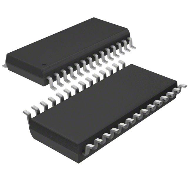
The CDCV855PW is a PLL Clock Driver IC manufactured by Texas Instruments, designed for clock distribution and timing applications requiring SSTL-2 signal levels. This device operates at a maximum frequency of 180MHz with a 1:5 input-to-output ratio and is housed in a 28-TSSOP surface mount package.
The CDCV855PW carries a "Not For New Designs" product status, indicating that Texas Instruments has discontinued active development for this component. This status necessitates identification of functionally equivalent alternatives for ongoing production requirements and new design implementations.
Substiute Parts
Key Parameters
| Parameter | Value |
|---|---|
| Manufacturer Part Number | CDCV855PW |
| Manufacturer | Texas Instruments |
| Category | Clock/Timing |
| Type | PLL Clock Driver |
| Package / Case | 28-TSSOP (0.173", 4.40mm Width) |
| Frequency - Max | 180MHz |
| Ratio - Input:Output | 1:5 |
| Input / Output Signal Level | SSTL-2 / SSTL-2 |
| Voltage - Supply | 2.3V ~ 2.7V |
| Operating Temperature | 0°C ~ 70°C |
| Mounting Type | Surface Mount |
| RoHS Status | ROHS3 Compliant |
| Moisture Sensitivity Level (MSL) | 1 (Unlimited) |
Substitute Part Grouping Explanation
Substitution eligibility for the CDCV855PW is determined by the following critical parameters:
- Package Compatibility: Identical 28-TSSOP (0.173", 4.40mm Width) surface mount package required for PCB layout compatibility
- Signal Level Compatibility: SSTL-2 input and output levels required for direct circuit integration
- Supply Voltage Range: 2.3V ~ 2.7V operating range required for power supply compatibility
- PLL Architecture: PLL with Bypass functionality required for functional equivalence
- Differential Signaling: Differential input and output capability required
- Number of Circuits: Single circuit configuration required
The CDCVF855PW qualifies as a direct substitute based on these parameters. While the CDCVF855PW exhibits higher maximum frequency (220MHz) and extended operating temperature range (-40°C ~ 85°C), these represent performance enhancements that do not compromise backward compatibility with CDCV855PW applications.
Parameter Comparison
| Parameter | CDCV855PW (Main Part) | CDCVF855PW (Substitute) |
|---|---|---|
| Manufacturer Part Number | CDCV855PW | CDCVF855PW |
| Manufacturer | Texas Instruments | Texas Instruments |
| Product Status | Not For New Designs | Active |
| Type | PLL Clock Driver | PLL Clock Driver |
| Package / Case | 28-TSSOP (0.173", 4.40mm Width) | 28-TSSOP (0.173", 4.40mm Width) |
| Frequency - Max | 180MHz | 220MHz |
| Ratio - Input:Output | 1:5 | 2:5 |
| Input Signal Level | SSTL-2 | SSTL-2 |
| Output Signal Level | SSTL-2 | SSTL-2 |
| Differential - Input/Output | Yes / Yes | Yes / Yes |
| Number of Circuits | 1 | 1 |
| Voltage - Supply | 2.3V ~ 2.7V | 2.3V ~ 2.7V |
| Operating Temperature | 0°C ~ 70°C | -40°C ~ 85°C |
| Mounting Type | Surface Mount | Surface Mount |
| RoHS Status | ROHS3 Compliant | ROHS3 Compliant |
| Moisture Sensitivity Level (MSL) | 1 (Unlimited) | 1 (Unlimited) |
Engineering Selection Recommendations
The CDCVF855PW is the recommended substitute for CDCV855PW applications. The CDCVF855PW maintains active product status with Texas Instruments, ensuring continued availability and manufacturing support. Both components meet ROHS3 compliance and REACH unaffected status, satisfying environmental and regulatory requirements.
The CDCVF855PW provides enhanced performance specifications including higher maximum frequency (220MHz versus 180MHz) and extended operating temperature range (-40°C ~ 85°C versus 0°C ~ 70°C). These improvements do not introduce compatibility issues for existing CDCV855PW designs, as the substitute operates within the same supply voltage range and maintains identical package and signal level specifications.
Frequently Asked Questions (FAQ)
Q: Can CDCVF855PW directly replace CDCV855PW in existing designs?
A: Yes. Both components share identical package geometry (28-TSSOP), supply voltage range (2.3V ~ 2.7V), and signal level specifications (SSTL-2 input/output). The CDCVF855PW operates at higher maximum frequency and extended temperature range, which do not create backward compatibility issues.
Q: What is the significance of the different input-to-output ratios (1:5 versus 2:5)?
A: The input-to-output ratio defines the frequency multiplication factor. CDCV855PW multiplies input frequency by 5, while CDCVF855PW multiplies by 2.5. Circuit design must account for this difference in frequency scaling when selecting the appropriate substitute.
Q: Are there package considerations for PCB redesign?
A: No. Both components use identical 28-TSSOP (0.173", 4.40mm Width) surface mount packaging. PCB footprints, land patterns, and assembly processes remain unchanged.
Q: Why is CDCV855PW marked "Not For New Designs"?
A: This designation indicates Texas Instruments has concluded active development for this component. CDCVF855PW represents the active product line continuation and is the appropriate selection for new designs and ongoing production.
Q: Are compliance certifications equivalent between the two parts?
A: Yes. Both CDCV855PW and CDCVF855PW maintain ROHS3 compliance and REACH unaffected status, satisfying identical environmental and regulatory requirements.
Alternative Parts

SJ6012L2TP
Littelfuse Inc.
6 Alternative Parts

JMK107BBJ476MA-RE
Taiyo Yuden
10 Alternative Parts

GMK107BBJ475MA-T
Taiyo Yuden
5 Alternative Parts
SJ6020N2ARP
Littelfuse Inc.
3 Alternative Parts
SJ6025R2ATP
Littelfuse Inc.
4 Alternative Parts

2474-05L
API Delevan Inc.
1 Alternative Parts

4590R-684K
API Delevan Inc.
1 Alternative Parts

CM6560R-334
API Delevan Inc.
1 Alternative Parts

CM6460-104
API Delevan Inc.
1 Alternative Parts

5526-12
API Delevan Inc.
1 Alternative Parts