


Request Quote
(Ships tomorrow)
CDCV855IPWG4 Equivalent & Substitute Parts
Part Overview
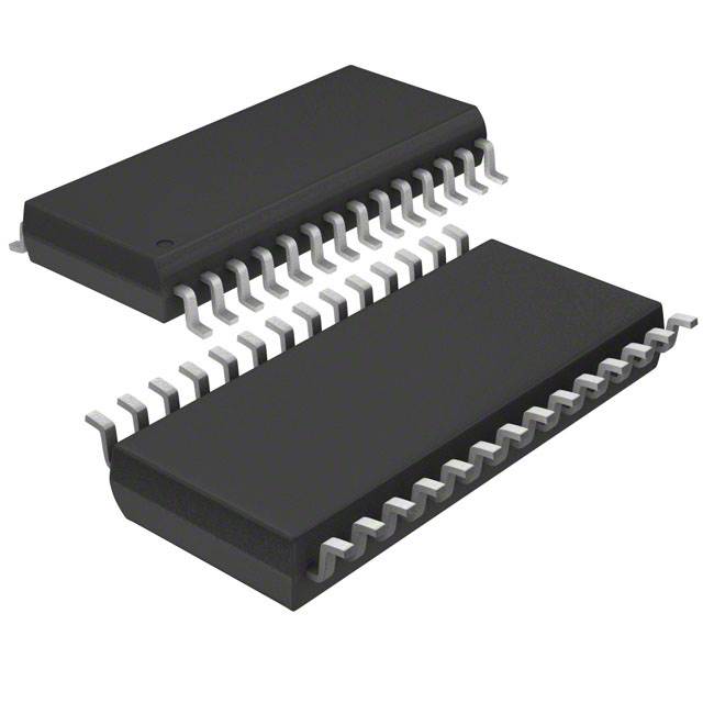
The CDCV855IPWG4 is a PLL Clock Driver IC manufactured by Texas Instruments, designed for clock distribution and timing applications requiring SSTL-2 signal levels. This device operates at a maximum frequency of 180MHz with a 1:5 input-to-output ratio and is housed in a 28-TSSOP surface mount package. The part is currently discontinued at DiGi Electronics, necessitating identification of equivalent alternatives for ongoing production and maintenance applications.
Substiute Parts
Key Parameters
| Parameter | Value |
|---|---|
| Manufacturer Part Number | CDCV855IPWG4 |
| Manufacturer | Texas Instruments |
| Category | Clock/Timing |
| Type | PLL Clock Driver |
| Package / Case | 28-TSSOP (0.173", 4.40mm Width) |
| Frequency - Max | 180MHz |
| Input / Output Signals | SSTL-2 / SSTL-2 |
| Ratio - Input:Output | 1:5 |
| Voltage - Supply | 2.3V ~ 2.7V |
| Operating Temperature | -40°C ~ 85°C |
| Mounting Type | Surface Mount |
| RoHS Status | ROHS3 Compliant |
| Moisture Sensitivity Level (MSL) | 1 (Unlimited) |
Substitute Part Grouping Explanation
Substitute parts for the CDCV855IPWG4 are identified based on compatibility across the following critical parameters:
- Package / Case: 28-TSSOP (0.173", 4.40mm Width) — mechanical and electrical interface compatibility
- Input / Output Signals: SSTL-2 / SSTL-2 — signal level compatibility
- Voltage - Supply: 2.3V ~ 2.7V — power supply compatibility
- Operating Temperature: -40°C ~ 85°C — thermal operating range
- Mounting Type: Surface Mount — assembly compatibility
- RoHS Status: ROHS3 Compliant — environmental compliance
- Moisture Sensitivity Level (MSL): 1 (Unlimited) — handling and storage compatibility
Substitute parts may differ in maximum frequency and input-to-output ratio while maintaining compatibility with the above parameters. Parts with higher frequency ratings or different multiplier ratios can serve as functional alternatives when circuit design permits.
Parameter Comparison
| Parameter | CDCV855IPWG4 | CDCVF855PW | CDCV855IPW |
|---|---|---|---|
| Manufacturer | Texas Instruments | Texas Instruments | Texas Instruments |
| Category | Clock/Timing | Clock/Timing | Clock/Timing |
| Type | PLL Clock Driver | PLL Clock Driver | PLL Clock Driver |
| Package / Case | 28-TSSOP (0.173", 4.40mm Width) | 28-TSSOP (0.173", 4.40mm Width) | 28-TSSOP (0.173", 4.40mm Width) |
| Frequency - Max | 180MHz | 220MHz | 180MHz |
| Input / Output Signals | SSTL-2 / SSTL-2 | SSTL-2 / SSTL-2 | SSTL-2 / SSTL-2 |
| Ratio - Input:Output | 1:5 | 2:5 | 1:5 |
| Voltage - Supply | 2.3V ~ 2.7V | 2.3V ~ 2.7V | 2.3V ~ 2.7V |
| Operating Temperature | -40°C ~ 85°C | -40°C ~ 85°C | -40°C ~ 85°C |
| Mounting Type | Surface Mount | Surface Mount | Surface Mount |
| RoHS Status | ROHS3 Compliant | ROHS3 Compliant | ROHS3 Compliant |
| Moisture Sensitivity Level (MSL) | 1 (Unlimited) | 1 (Unlimited) | 1 (Unlimited) |
| Product Status | Discontinued at DiGi Electronics | Active | Not For New Designs |
Engineering Selection Recommendations
CDCVF855PW is the primary active substitute for CDCV855IPWG4. This part maintains full compatibility across all critical electrical and mechanical parameters, including package, signal levels, supply voltage, and operating temperature range. The CDCVF855PW offers an increased maximum frequency of 220MHz and a different input-to-output ratio of 2:5 compared to the original 1:5 ratio. The part is currently in active production status and carries ROHS3 compliance certification.
CDCV855IPW is an alternative substitute that maintains identical electrical specifications to CDCV855IPWG4, including the 1:5 input-to-output ratio and 180MHz maximum frequency. However, this part is designated as "Not For New Designs" by the manufacturer, making it suitable only for legacy system maintenance and repair applications where exact parameter matching is required.
For new designs, CDCVF855PW is the recommended selection due to its active product status and higher frequency capability. For legacy system support requiring exact parameter matching, CDCV855IPW provides functional equivalence despite its discontinued design status.
Frequently Asked Questions (FAQ)
Q: Can CDCVF855PW directly replace CDCV855IPWG4 in existing designs?
A: CDCVF855PW is mechanically and electrically compatible with CDCV855IPWG4 across all critical parameters including package, signal levels, supply voltage, and operating temperature. However, the different input-to-output ratio (2:5 versus 1:5) and higher maximum frequency (220MHz versus 180MHz) must be evaluated within the specific circuit application to ensure functional compatibility.
Q: What is the difference between CDCV855IPW and CDCVF855PW?
A: Both parts are compatible with CDCV855IPWG4 in terms of package and signal levels. CDCV855IPW maintains identical frequency and ratio specifications (180MHz, 1:5), while CDCVF855PW offers higher frequency capability (220MHz) with a different ratio (2:5). CDCVF855PW is in active production; CDCV855IPW is not recommended for new designs.
Q: Are all substitute parts in the same 28-TSSOP package?
A: Yes. CDCV855IPWG4, CDCVF855PW, and CDCV855IPW are all housed in the 28-TSSOP (0.173", 4.40mm Width) surface mount package, ensuring mechanical compatibility and identical PCB footprint requirements.
Q: Do all parts meet the same environmental compliance standards?
A: Yes. CDCV855IPWG4, CDCVF855PW, and CDCV855IPW are all ROHS3 compliant with Moisture Sensitivity Level 1 (Unlimited), ensuring equivalent environmental and handling requirements.
Q: What supply voltage range is required for these parts?
A: All three parts operate within the 2.3V to 2.7V supply voltage range and maintain the same operating temperature specification of -40°C to 85°C.
Alternative Parts

SJ6012L2TP
Littelfuse Inc.
6 Alternative Parts

JMK107BBJ476MA-RE
Taiyo Yuden
10 Alternative Parts

GMK107BBJ475MA-T
Taiyo Yuden
5 Alternative Parts
SJ6020N2ARP
Littelfuse Inc.
3 Alternative Parts
SJ6025R2ATP
Littelfuse Inc.
4 Alternative Parts

2474-05L
API Delevan Inc.
1 Alternative Parts

4590R-684K
API Delevan Inc.
1 Alternative Parts

CM6560R-334
API Delevan Inc.
1 Alternative Parts

CM6460-104
API Delevan Inc.
1 Alternative Parts

5526-12
API Delevan Inc.
1 Alternative Parts