


Request Quote
(Ships tomorrow)
CDCU877ZQLR Equivalent & Substitute Parts
Part Overview
The CDCU877ZQLR is a Memory DDR2 Clock Buffer/Driver IC manufactured by Texas Instruments, designed for high-speed clock distribution in DDR2 memory applications. This device features a 1:10 input-to-output ratio with differential signaling on both input and output, operating at frequencies up to 400MHz with 1.8V supply voltage compatibility.
The CDCU877ZQLR is classified as obsolete. Identifying suitable substitute parts is necessary to maintain design continuity and ensure availability for new production runs, system upgrades, or replacement inventory requirements.
Substiute Parts
Key Parameters
| Parameter | Value |
|---|---|
| Manufacturer Part Number | CDCU877ZQLR |
| Manufacturer | Texas Instruments |
| Category | Clock/Timing |
| Product Type | Memory DDR2 Clock Buffer/Driver, Multiplexer IC |
| Frequency - Max | 400MHz |
| Voltage - Supply | 1.7V ~ 1.9V |
| Number of Circuits | 1 |
| Ratio - Input:Output | 1:10 |
| Differential - Input:Output | Yes/Yes |
| Input Signal Type | SSTL-18 |
| Output Signal Type | SSTL-18 |
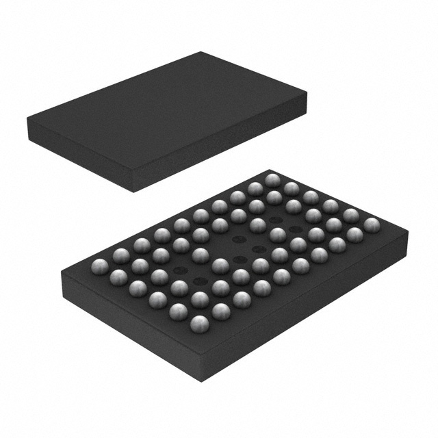
| Package / Case | 52-VFBGA |
| Mounting Type | Surface Mount |
| Operating Temperature Range | -40°C ~ 85°C |
| RoHS Status | ROHS3 Compliant |
| Moisture Sensitivity Level (MSL) | 2 (1 Year) |
| Product Status | Obsolete |
Substitute Part Grouping Explanation
Substitute parts for the CDCU877ZQLR must satisfy the following critical parameters to ensure functional and mechanical compatibility:
Mandatory Matching Parameters:
- Package type: 52-VFBGA (52-pin Very Fine Ball Grid Array)
- Mounting type: Surface Mount
- Functional category: Memory DDR2 Clock Buffer/Driver with Multiplexer capability
- Input-to-output ratio: 1:10
- Differential signaling: Yes on both input and output
- Supply voltage range: 1.7V ~ 1.9V (1.8V nominal)
- Output signal type: SSTL-18
Allowable Parameter Variations:
- Maximum frequency: Equal to or greater than 400MHz
- Operating temperature range: May be narrower than the original specification
- Product status: Active or Obsolete (availability dependent)
- RoHS and MSL compliance: May differ based on manufacturing date and regional requirements
The 98ULPA877AHT from Renesas Electronics Corporation qualifies as a substitute based on these criteria.
Parameter Comparison
| Parameter | CDCU877ZQLR (Texas Instruments) | 98ULPA877AHT (Renesas Electronics) | Compatibility |
|---|---|---|---|
| Category | Clock/Timing | Clock/Timing | Match |
| Product Type | Memory DDR2 Clock Buffer/Driver, Multiplexer IC | Memory DDR2 Clock Buffer/Driver, Zero Delay Buffer, Multiplexer IC | Compatible |
| Frequency - Max | 400MHz | 410MHz | Substitute exceeds specification |
| Voltage - Supply | 1.7V ~ 1.9V | 1.7V ~ 1.9V | Match |
| Number of Circuits | 1 | 1 | Match |
| Ratio - Input:Output | 1:10 | 1:10 | Match |
| Differential - Input:Output | Yes/Yes | Yes/Yes | Match |
| Output Signal Type | SSTL-18 | SSTL-18 | Match |
| Package / Case | 52-VFBGA | 52-VFBGA | Match |
| Supplier Device Package | 52-BGA MICROSTAR JUNIOR (7x4.5) | 52-CABGA (4.5x7.0) | Equivalent footprint |
| Mounting Type | Surface Mount | Surface Mount | Match |
| Operating Temperature Range | -40°C ~ 85°C | 0°C ~ 70°C | Substitute has narrower range |
| RoHS Status | ROHS3 Compliant | RoHS non-compliant | Difference in compliance |
| Moisture Sensitivity Level (MSL) | 2 (1 Year) | 3 (168 Hours) | Substitute requires stricter handling |
| Product Status | Obsolete | Active | Substitute is currently manufactured |
Engineering Selection Recommendations
Availability Consideration: The CDCU877ZQLR is obsolete and no longer manufactured by Texas Instruments. The 98ULPA877AHT is an active product from Renesas Electronics Corporation with current production inventory, making it the primary substitute option for new designs or replacement stock requirements.
Compliance Considerations: The original CDCU877ZQLR is ROHS3 compliant. The 98ULPA877AHT is RoHS non-compliant. Organizations subject to RoHS regulations must evaluate whether this substitution aligns with procurement and environmental compliance policies.
Operating Temperature Range: The CDCU877ZQLR operates across -40°C to 85°C, while the 98ULPA877AHT operates across 0°C to 70°C. Applications requiring extended low-temperature operation below 0°C or high-temperature operation above 70°C cannot use the Renesas substitute without design modification or thermal management review.
Moisture Sensitivity: The CDCU877ZQLR has MSL 2 (1 Year shelf life), while the 98ULPA877AHT has MSL 3 (168 Hours shelf life). The substitute requires more stringent moisture control during storage and handling. Procurement and assembly processes must accommodate the shorter bake-out window.
Frequency Performance: The 98ULPA877AHT operates at 410MHz maximum, exceeding the 400MHz specification of the CDCU877ZQLR. This performance margin provides additional headroom for clock distribution applications.
Frequently Asked Questions (FAQ)
Q: Can the 98ULPA877AHT be used as a direct replacement for the CDCU877ZQLR in existing designs?
A: The 98ULPA877AHT is functionally compatible at the circuit level, sharing identical package footprint (52-VFBGA), supply voltage (1.7V ~ 1.9V), input-to-output ratio (1:10), and differential signaling characteristics. However, three factors require evaluation: (1) operating temperature range is narrower (0°C to 70°C versus -40°C to 85°C), (2) RoHS compliance differs, and (3) moisture sensitivity level is higher (MSL 3 versus MSL 2). Designs operating within 0°C to 70°C and compatible with RoHS non-compliant components can use this substitute without circuit modification.
Q: What is the difference between the MICROSTAR JUNIOR and CABGA package designations?
A: Both designations refer to 52-pin ball grid array packages with equivalent footprints (7x4.5mm and 4.5x7.0mm are the same physical dimensions, rotated). The MICROSTAR JUNIOR is Texas Instruments' package designation, while CABGA is Renesas Electronics' designation. The physical layout, ball pitch, and PCB footprint are compatible.
Q: Are there any signal integrity differences between these two clock drivers?
A: Both devices support SSTL-18 input and output signaling with differential pairs on both sides. The 98ULPA877AHT includes zero-delay buffer functionality, which may provide improved timing characteristics compared to the CDCU877ZQLR. Timing specifications should be reviewed against application requirements.
Q: What handling precautions apply to the 98ULPA877AHT due to its higher MSL rating?
A: MSL 3 (168 Hours) requires that the component be baked at 125°C for 24 hours if exposed to moisture for more than 168 hours before assembly. The CDCU877ZQLR with MSL 2 (1 Year) allows longer shelf life without baking. Assembly facilities must implement moisture control procedures and track component exposure time accordingly.
Q: Is the 410MHz maximum frequency of the 98ULPA877AHT sufficient for DDR2 applications designed for 400MHz?
A: Yes. The 410MHz specification exceeds the 400MHz requirement, providing a 2.5% performance margin. This additional headroom is acceptable for DDR2 clock distribution applications.
Q: What is the REACH status for both parts?
A: Both the CDCU877ZQLR and 98ULPA877AHT are listed as REACH Unaffected, indicating they are not subject to REACH substance restrictions.
Alternative Parts

SJ6012L2TP
Littelfuse Inc.
6 Alternative Parts

JMK107BBJ476MA-RE
Taiyo Yuden
10 Alternative Parts

GMK107BBJ475MA-T
Taiyo Yuden
5 Alternative Parts
SJ6020N2ARP
Littelfuse Inc.
3 Alternative Parts
SJ6025R2ATP
Littelfuse Inc.
4 Alternative Parts

2474-05L
API Delevan Inc.
1 Alternative Parts

4590R-684K
API Delevan Inc.
1 Alternative Parts

CM6560R-334
API Delevan Inc.
1 Alternative Parts

CM6460-104
API Delevan Inc.
1 Alternative Parts

5526-12
API Delevan Inc.
1 Alternative Parts