


Request Quote
(Ships tomorrow)
CDCU877AGQLR Equivalent & Substitute Parts
Part Overview
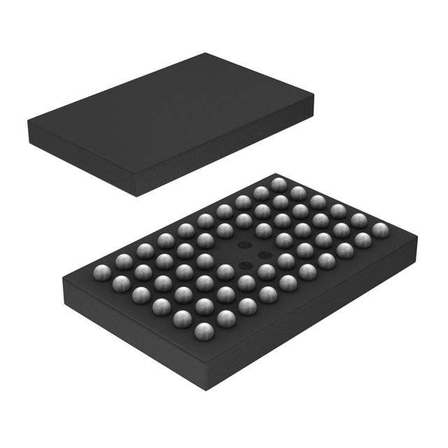
The CDCU877AGQLR is a Memory DDR2 Clock Buffer/Driver IC manufactured by Texas Instruments, designed for high-speed clock distribution in DDR2 memory applications. This 56-BGA device operates at up to 400MHz with 1.8V supply voltage and provides single output with 1:10 input-to-output ratio. The product is currently obsolete, making identification of compatible substitute parts essential for system redesign, legacy support, or inventory replacement scenarios.
Substiute Parts
Key Parameters
| Parameter | Value |
|---|---|
| Manufacturer Part Number | CDCU877AGQLR |
| Manufacturer | Texas Instruments |
| Category | Clock/Timing |
| Product Status | Obsolete |
| Main Purpose | Memory, DDR2 |
| Frequency - Max | 400MHz |
| Voltage - Supply | 1.7V ~ 1.9V |
| Number of Circuits | 1 |
| Ratio - Input:Output | 1:10 |
| Differential - Input:Output | Yes/Yes |
| Input Signal Type | SSTL-18 |
| Output Signal Type | SSTL-18 |
| Package / Case | 56-VFBGA |
| Operating Temperature | -40°C ~ 85°C |
| Mounting Type | Surface Mount |
| PLL | Yes |
| RoHS Status | RoHS non-compliant |
| Moisture Sensitivity Level (MSL) | 2 (1 Year) |
Substitute Part Grouping Explanation
Substitution eligibility for the CDCU877AGQLR is determined by the following critical parameters:
Core Functional Requirements:
- Main Purpose: Memory, DDR2 clock distribution
- Number of Circuits: 1 output channel
- Ratio - Input:Output: 1:10 multiplication factor
- Differential signaling: Yes for both input and output
- Signal Type: SSTL-18 compatible input and output
Electrical Compatibility:
- Voltage - Supply: 1.7V ~ 1.9V operating range
- Frequency - Max: Minimum 400MHz capability
- PLL: Required for clock generation
Physical Compatibility:
- Mounting Type: Surface Mount
- Package Type: BGA (Ball Grid Array) format
- Pin count and footprint: Must accommodate 56-pin or compatible BGA configuration
The substitute part 98ULPA877AHT from Renesas Electronics Corporation meets these core functional and electrical requirements, with the following considerations noted in the parameter comparison section.
Parameter Comparison
| Parameter | CDCU877AGQLR (Texas Instruments) | 98ULPA877AHT (Renesas Electronics) |
|---|---|---|
| Category | Clock/Timing | Clock/Timing |
| Main Purpose | Memory, DDR2 | Memory, DDR2 |
| Frequency - Max | 400MHz | 410MHz |
| Voltage - Supply | 1.7V ~ 1.9V | 1.7V ~ 1.9V |
| Number of Circuits | 1 | 1 |
| Ratio - Input:Output | 1:10 | 1:10 |
| Differential - Input:Output | Yes/Yes | Yes/Yes |
| Output Signal Type | SSTL-18 | SSTL-18 |
| Mounting Type | Surface Mount | Surface Mount |
| Package / Case | 56-VFBGA | 52-VFBGA |
| Operating Temperature | -40°C ~ 85°C | 0°C ~ 70°C |
| Product Status | Obsolete | Active |
| PLL | Yes | Yes |
| RoHS Status | RoHS non-compliant | RoHS non-compliant |
| Moisture Sensitivity Level (MSL) | 2 (1 Year) | 3 (168 Hours) |
Engineering Selection Recommendations
The 98ULPA877AHT from Renesas Electronics Corporation is identified as a manufacturer-recommended substitute for the obsolete CDCU877AGQLR. Both devices share identical electrical specifications for supply voltage (1.7V ~ 1.9V), input-to-output ratio (1:10), differential signaling capability, and SSTL-18 signal compatibility.
Key Considerations:
The substitute part operates at a higher maximum frequency (410MHz versus 400MHz), providing performance margin for DDR2 clock distribution applications. Both parts maintain RoHS non-compliant status and REACH unaffected compliance classification.
Differences Requiring Attention:
The 98ULPA877AHT operates within a narrower temperature range (0°C ~ 70°C) compared to the original part (-40°C ~ 85°C). Applications requiring extended temperature operation below 0°C or above 70°C must evaluate this limitation against system requirements.
The package configuration differs: the substitute uses 52-VFBGA (4.5x7.0mm) versus the original 56-VFBGA. This package change requires PCB layout verification to confirm footprint compatibility and signal integrity.
Moisture sensitivity level increases from MSL 2 (1 Year) to MSL 3 (168 Hours), requiring adjusted handling and storage protocols during manufacturing and assembly.
The substitute part is currently in active production status, ensuring availability for new designs and legacy system support.
Frequently Asked Questions (FAQ)
Q: Can the 98ULPA877AHT directly replace the CDCU877AGQLR without PCB modifications?
A: Package differences (56-VFBGA to 52-VFBGA) require PCB footprint verification. The ball grid array dimensions differ (7x4.5mm to 4.5x7.0mm), necessitating layout review before implementation.
Q: What is the impact of the narrower operating temperature range on system design?
A: The substitute part operates from 0°C to 70°C, compared to the original -40°C to 85°C range. Applications requiring operation below 0°C or above 70°C must confirm compatibility with actual system thermal requirements.
Q: Are the electrical specifications identical between the two parts?
A: Yes. Both devices provide 1:10 clock multiplication, SSTL-18 differential input and output, 1.7V ~ 1.9V supply voltage, and single-circuit configuration. The substitute operates at 410MHz maximum frequency, exceeding the original 400MHz specification.
Q: What changes are required for handling and storage?
A: The substitute part has MSL 3 (168 Hours) moisture sensitivity versus MSL 2 (1 Year) for the original. This requires stricter moisture control during storage and reduced time-to-assembly windows. Baking procedures may be necessary if moisture absorption limits are exceeded.
Q: Is the substitute part suitable for new DDR2 clock distribution designs?
A: Yes. The 98ULPA877AHT is in active production status and meets all functional requirements for DDR2 memory clock buffer applications. The higher maximum frequency provides design margin for high-speed memory systems.
Q: How do the package dimensions affect signal integrity?
A: Both packages are BGA format with similar ball pitch. The dimensional change (7x4.5mm to 4.5x7.0mm) may affect trace routing and via placement. Signal integrity analysis should be performed during PCB layout verification to confirm compliance with system timing requirements.
Alternative Parts

SJ6012L2TP
Littelfuse Inc.
6 Alternative Parts

JMK107BBJ476MA-RE
Taiyo Yuden
10 Alternative Parts

GMK107BBJ475MA-T
Taiyo Yuden
5 Alternative Parts
SJ6020N2ARP
Littelfuse Inc.
3 Alternative Parts
SJ6025R2ATP
Littelfuse Inc.
4 Alternative Parts

2474-05L
API Delevan Inc.
1 Alternative Parts

4590R-684K
API Delevan Inc.
1 Alternative Parts

CM6560R-334
API Delevan Inc.
1 Alternative Parts

CM6460-104
API Delevan Inc.
1 Alternative Parts

5526-12
API Delevan Inc.
1 Alternative Parts