


Request Quote
(Ships tomorrow)
CDCLVD110AVFR Equivalent & Substitute Parts
Part Overview
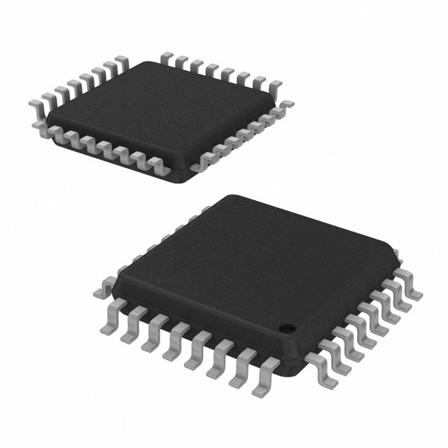
The CDCLVD110AVFR is a Clock Fanout Buffer (Distribution) Multiplexer IC manufactured by Texas Instruments, designed for high-speed clock distribution applications. This device features a 2:10 input-to-output ratio with LVDS (Low-Voltage Differential Signaling) on both input and output, supporting frequencies up to 1.1 GHz. The part is currently in Active product status with 3554 units available in stock.
Finding equivalent and substitute parts becomes necessary when the primary part reaches end-of-life status, inventory constraints occur, or design flexibility is required for supply chain optimization. The CDCLVD110VFR serves as a parametric equivalent with identical electrical and mechanical specifications, though it carries a Not For New Designs status.
Substiute Parts
Key Parameters
| Parameter | Value |
|---|---|
| Manufacturer | Texas Instruments |
| Part Number | CDCLVD110AVFR |
| Category | Clock/Timing |
| Type | Fanout Buffer (Distribution), Multiplexer |
| Ratio - Input:Output | 2:10 |
| Input Signal Type | LVDS |
| Output Signal Type | LVDS |
| Frequency - Max | 1.1 GHz |
| Voltage - Supply | 2.375V ~ 2.625V |
| Operating Temperature Range | -40°C ~ 85°C |
| Package / Case | 32-LQFP (7x7) |
| Mounting Type | Surface Mount |
| RoHS Status | ROHS3 Compliant |
| Moisture Sensitivity Level (MSL) | 1 (Unlimited) |
| Product Status | Active |
Substitute Part Grouping Explanation
Substitution of the CDCLVD110AVFR is determined by strict adherence to the following electrical and mechanical parameters:
Critical Substitution Parameters:
- Input-to-Output Ratio: 2:10
- Input Signal Type: LVDS
- Output Signal Type: LVDS
- Maximum Frequency: 1.1 GHz
- Supply Voltage Range: 2.375V ~ 2.625V
- Operating Temperature Range: -40°C ~ 85°C
- Package Type: 32-LQFP (7x7)
- Mounting Type: Surface Mount
The CDCLVD110VFR is classified as a parametric equivalent because it matches all electrical specifications and mechanical parameters of the CDCLVD110AVFR. The primary distinction is product lifecycle status: CDCLVD110AVFR is Active, while CDCLVD110VFR is designated Not For New Designs.
Parameter Comparison
| Parameter | CDCLVD110AVFR (Main) | CDCLVD110VFR (Substitute) |
|---|---|---|
| Manufacturer | Texas Instruments | Texas Instruments |
| Category | Clock/Timing | Clock/Timing |
| Type | Fanout Buffer (Distribution), Multiplexer | Fanout Buffer (Distribution), Multiplexer |
| Ratio - Input:Output | 2:10 | 2:10 |
| Input Signal Type | LVDS | LVDS |
| Output Signal Type | LVDS | LVDS |
| Frequency - Max | 1.1 GHz | 1.1 GHz |
| Voltage - Supply | 2.375V ~ 2.625V | 2.375V ~ 2.625V |
| Operating Temperature Range | -40°C ~ 85°C | -40°C ~ 85°C |
| Package / Case | 32-LQFP (7x7) | 32-LQFP (7x7) |
| Mounting Type | Surface Mount | Surface Mount |
| RoHS Status | ROHS3 Compliant | ROHS3 Compliant |
| Moisture Sensitivity Level (MSL) | 1 (Unlimited) | 1 (Unlimited) |
| Product Status | Active | Not For New Designs |
| Inventory | 3554 Pcs | 1153 Pcs |
Engineering Selection Recommendations
For Active Designs: The CDCLVD110AVFR is the preferred selection due to its Active product status, ensuring long-term availability and continued manufacturer support. This part carries full compliance certifications including ROHS3, REACH Unaffected status, and unlimited moisture sensitivity rating.
For Existing Designs Using CDCLVD110VFR: The CDCLVD110VFR remains functionally equivalent and electrically interchangeable with the CDCLVD110AVFR. However, the Not For New Designs designation indicates this part is in end-of-life phase. Existing inventory of 1153 units is available, but migration to the CDCLVD110AVFR is recommended for long-term supply chain stability.
Compliance Considerations: Both parts maintain identical compliance profiles: ROHS3 Compliant, REACH Unaffected, and EAR99 export classification. MSL rating of 1 (Unlimited) indicates no moisture sensitivity constraints for storage or handling.
Frequently Asked Questions (FAQ)
Q: Can CDCLVD110VFR be used as a direct replacement for CDCLVD110AVFR?
A: Yes. The CDCLVD110VFR is electrically and mechanically identical to the CDCLVD110AVFR across all specified parameters: 2:10 LVDS fanout buffer, 1.1 GHz maximum frequency, 2.375V–2.625V supply voltage, 32-LQFP package, and -40°C to 85°C operating range. The only distinction is product lifecycle status.
Q: What does "Not For New Designs" mean for the CDCLVD110VFR?
A: This designation indicates the part is in end-of-life phase and Texas Instruments does not recommend its use in new product designs. Existing inventory may be available for legacy system support or design continuation, but new designs should utilize the CDCLVD110AVFR.
Q: Are there any package or pinout differences between these parts?
A: No. Both parts use identical 32-LQFP (7x7) surface mount packaging with the same pinout configuration. PCB layout and footprint are fully compatible.
Q: What are the compliance and environmental certifications for these parts?
A: Both CDCLVD110AVFR and CDCLVD110VFR are ROHS3 Compliant, REACH Unaffected, and carry MSL rating of 1 (Unlimited), indicating no moisture sensitivity restrictions. Both are classified under ECCN EAR99 for export purposes.
Q: Which part should be selected for a new clock distribution design?
A: The CDCLVD110AVFR should be selected for new designs due to its Active product status, ensuring manufacturer support and long-term availability. The CDCLVD110VFR is suitable only for legacy system maintenance or design continuation where existing inventory is available.
Alternative Parts

SJ6012L2TP
Littelfuse Inc.
6 Alternative Parts

JMK107BBJ476MA-RE
Taiyo Yuden
10 Alternative Parts

GMK107BBJ475MA-T
Taiyo Yuden
5 Alternative Parts
SJ6020N2ARP
Littelfuse Inc.
3 Alternative Parts
SJ6025R2ATP
Littelfuse Inc.
4 Alternative Parts

2474-05L
API Delevan Inc.
1 Alternative Parts

4590R-684K
API Delevan Inc.
1 Alternative Parts

CM6560R-334
API Delevan Inc.
1 Alternative Parts

CM6460-104
API Delevan Inc.
1 Alternative Parts

5526-12
API Delevan Inc.
1 Alternative Parts