


Request Quote
(Ships tomorrow)
CDCLVC1110PWR Clock Fanout Buffer Equivalent & Substitute Parts
Part Overview
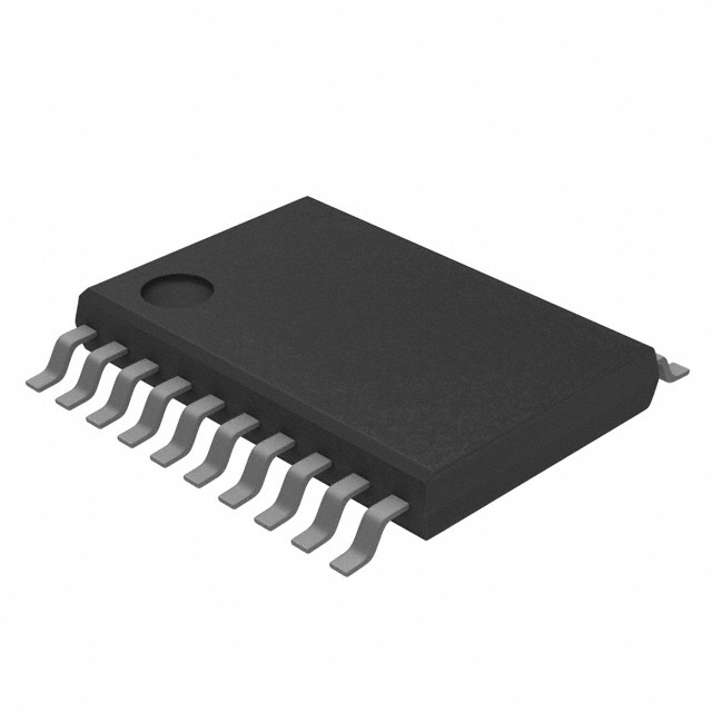
The CDCLVC1110PWR is an active Clock Fanout Buffer (Distribution) IC manufactured by Texas Instruments, designed for 1:10 clock distribution applications with a maximum frequency of 250 MHz. This component operates across a supply voltage range of 2.3V to 3.6V and is housed in a 20-TSSOP surface mount package. The part maintains Active product status and is RoHS3 compliant with unlimited moisture sensitivity level (MSL 1).
Substitute parts become necessary when the primary component experiences supply constraints, extended lead times, or when alternative packaging formats (Tube or Tape & Reel) are required for specific manufacturing workflows.
Substiute Parts
Key Parameters
| Parameter | Value |
|---|---|
| Manufacturer Part Number | CDCLVC1110PWR |
| Manufacturer | Texas Instruments |
| Category | Clock/Timing |
| Type | Fanout Buffer (Distribution) |
| Ratio - Input:Output | 1:10 |
| Input/Output Type | LVCMOS / LVCMOS |
| Frequency - Max | 250 MHz |
| Voltage - Supply | 2.3V ~ 3.6V |
| Operating Temperature | -40°C ~ 85°C |
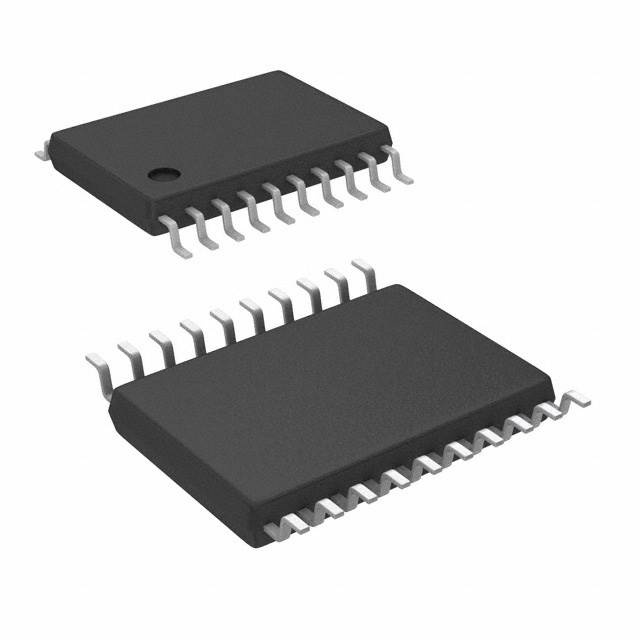
| Package / Case | 20-TSSOP (0.173", 4.40mm Width) |
| Mounting Type | Surface Mount |
| Product Status | Active |
| RoHS Status | ROHS3 Compliant |
| MSL Rating | 1 (Unlimited) |
Substitute Part Grouping Explanation
Substitute parts for the CDCLVC1110PWR are qualified based on the following critical parameters that determine functional and mechanical compatibility:
Mandatory Matching Parameters:
- Ratio - Input:Output: 1:10
- Input/Output Logic Type: LVCMOS / LVCMOS
- Package / Case: 20-TSSOP (0.173", 4.40mm Width)
- Mounting Type: Surface Mount
- Operating Temperature Range: -40°C ~ 85°C
- Product Status: Active
Allowable Variation Parameters:
- Frequency - Max: The substitute may operate at a lower maximum frequency than the primary part, provided it meets or exceeds the application requirement
- Voltage - Supply: The substitute voltage range may differ, provided the application supply voltage falls within the substitute's specified range
- Packaging Format: Cut Tape (CT), Tube, or Tape & Reel (TR) formats are interchangeable for the same component
The identified substitutes (5PB1110PGGI and 5PB1110PGGI8) maintain identical 1:10 fanout ratios, LVCMOS input/output characteristics, and 20-TSSOP package specifications. Both operate across the required -40°C to 85°C temperature range and maintain Active product status with RoHS3 compliance.
Parameter Comparison
| Parameter | CDCLVC1110PWR (TI) | 5PB1110PGGI (Renesas) | 5PB1110PGGI8 (Renesas) |
|---|---|---|---|
| Manufacturer | Texas Instruments | Renesas Electronics Corporation | Renesas Electronics Corporation |
| Type | Fanout Buffer (Distribution) | Fanout Buffer (Distribution) | Fanout Buffer (Distribution) |
| Ratio - Input:Output | 1:10 | 1:10 | 1:10 |
| Input/Output Type | LVCMOS / LVCMOS | LVCMOS / LVCMOS | LVCMOS / LVCMOS |
| Frequency - Max | 250 MHz | 200 MHz | 200 MHz |
| Voltage - Supply | 2.3V ~ 3.6V | 1.71V ~ 3.465V | 1.71V ~ 3.465V |
| Operating Temperature | -40°C ~ 85°C | -40°C ~ 85°C | -40°C ~ 85°C |
| Package / Case | 20-TSSOP (0.173", 4.40mm Width) | 20-TSSOP (0.173", 4.40mm Width) | 20-TSSOP (0.173", 4.40mm Width) |
| Mounting Type | Surface Mount | Surface Mount | Surface Mount |
| Product Status | Active | Active | Active |
| RoHS Status | ROHS3 Compliant | ROHS3 Compliant | ROHS3 Compliant |
| MSL Rating | 1 (Unlimited) | 1 (Unlimited) | 1 (Unlimited) |
| Packaging Format | Cut Tape (CT) & Digi-Reel® | Tube | Tape & Reel (TR) |
Engineering Selection Recommendations
Primary Part (CDCLVC1110PWR): Select the Texas Instruments CDCLVC1110PWR when maximum frequency performance of 250 MHz is required and supply voltage remains within the 2.3V to 3.6V range. This part is Active, RoHS3 compliant, and available in Cut Tape and Digi-Reel packaging formats.
Substitute Part 5PB1110PGGI (Renesas, Tube Packaging): The 5PB1110PGGI is suitable when the application frequency requirement does not exceed 200 MHz and the supply voltage falls within the 1.71V to 3.465V range. This part is Active, RoHS3 compliant, and packaged in Tube format. Select this variant when Tube packaging aligns with manufacturing processes.
Substitute Part 5PB1110PGGI8 (Renesas, Tape & Reel Packaging): The 5PB1110PGGI8 is suitable when the application frequency requirement does not exceed 200 MHz and the supply voltage falls within the 1.71V to 3.465V range. This part is Active, RoHS3 compliant, and packaged in Tape & Reel format. Select this variant when Tape & Reel packaging is required for automated assembly processes.
All three parts maintain identical 1:10 fanout ratios, LVCMOS logic compatibility, 20-TSSOP package dimensions, and -40°C to 85°C operating temperature specifications.
Frequently Asked Questions (FAQ)
Q: Can the Renesas 5PB1110PGGI or 5PB1110PGGI8 directly replace the Texas Instruments CDCLVC1110PWR?
A: Direct replacement is possible when the application frequency requirement does not exceed 200 MHz. Both Renesas substitutes maintain the identical 1:10 fanout ratio, LVCMOS input/output characteristics, and 20-TSSOP package footprint. The primary difference is the maximum frequency specification (200 MHz versus 250 MHz). If your circuit operates below 200 MHz, substitution is functionally compatible.
Q: What is the difference between 5PB1110PGGI and 5PB1110PGGI8?
A: Both parts are electrically identical Renesas clock fanout buffers with 1:10 distribution, 200 MHz maximum frequency, and identical electrical specifications. The difference is packaging format: 5PB1110PGGI is supplied in Tube packaging, while 5PB1110PGGI8 is supplied in Tape & Reel format. Select based on your manufacturing assembly requirements.
Q: Are the voltage supply ranges compatible across all three parts?
A: The voltage ranges differ slightly. The CDCLVC1110PWR operates from 2.3V to 3.6V, while both Renesas substitutes operate from 1.71V to 3.465V. If your application uses a supply voltage between 2.3V and 3.465V, all three parts are compatible. If your supply is below 2.3V or above 3.465V, verify compatibility with the specific part's datasheet.
Q: Does the 20-TSSOP package footprint remain identical across all substitutes?
A: Yes. All three parts use the 20-TSSOP package with 0.173" width and 4.40mm body width. PCB footprints and land patterns are identical, allowing direct board-level substitution without layout modifications.
Q: What compliance certifications apply to all substitute parts?
A: All three parts are RoHS3 compliant, REACH unaffected, and carry MSL 1 (Unlimited) moisture sensitivity ratings. All maintain Active product status. ECCN classification is EAR99 for all parts, and HTSUS code is 8542.39.0001.
Q: If my application requires 250 MHz operation, can I use the Renesas substitutes?
A: No. The Renesas 5PB1110PGGI and 5PB1110PGGI8 are specified for maximum 200 MHz operation. If your circuit requires 250 MHz performance, the Texas Instruments CDCLVC1110PWR is the appropriate selection.
Alternative Parts

SJ6012L2TP
Littelfuse Inc.
6 Alternative Parts

JMK107BBJ476MA-RE
Taiyo Yuden
10 Alternative Parts

GMK107BBJ475MA-T
Taiyo Yuden
5 Alternative Parts
SJ6020N2ARP
Littelfuse Inc.
3 Alternative Parts
SJ6025R2ATP
Littelfuse Inc.
4 Alternative Parts

2474-05L
API Delevan Inc.
1 Alternative Parts

4590R-684K
API Delevan Inc.
1 Alternative Parts

CM6560R-334
API Delevan Inc.
1 Alternative Parts

CM6460-104
API Delevan Inc.
1 Alternative Parts

5526-12
API Delevan Inc.
1 Alternative Parts