


Request Quote
(Ships tomorrow)
CDCF2510PW Equivalent & Substitute Parts
Part Overview
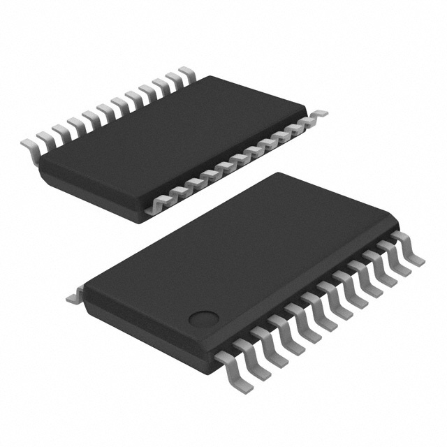
The CDCF2510PW is a 3.3V PLL Clock Driver IC manufactured by Texas Instruments, designed for memory and DRAM DIMM clock buffering and driving applications. This 24-TSSOP surface mount device operates at a maximum frequency of 140MHz with a 1:10 input-to-output ratio and supports single output configuration.
The CDCF2510PW is classified as obsolete. Identifying equivalent substitute parts is necessary to maintain design continuity, ensure supply chain availability, and support ongoing production requirements for systems utilizing this clock driver architecture.
Substiute Parts
Key Parameters
| Parameter | Value |
|---|---|
| Manufacturer Part Number | CDCF2510PW |
| Manufacturer | Texas Instruments |
| Category | Clock/Timing |
| Description | IC 3.3V PLL CLOCK-DRVR 24-TSSOP |
| Package / Case | 24-TSSOP (0.173", 4.40mm Width) |
| Frequency - Max | 140MHz |
| Voltage - Supply | 3V ~ 3.6V |
| Operating Temperature | 0°C ~ 85°C |
| Mounting Type | Surface Mount |
| Number of Circuits | 1 |
| Ratio - Input:Output | 1:10 |
| Product Status | Obsolete |
| RoHS Status | ROHS3 Compliant |
| Moisture Sensitivity Level (MSL) | 1 (Unlimited) |
Substitute Part Grouping Explanation
Substitution eligibility for the CDCF2510PW is determined by the following critical parameters:
- Package compatibility: 24-TSSOP form factor with identical 0.173" (4.40mm) width
- Supply voltage range: 3V to 3.6V operation
- Operating temperature range: 0°C to 85°C
- PLL functionality: Clock driver with phase-locked loop capability
- Single output circuit configuration
- Surface mount technology
- Compliance certifications: ROHS3, MSL Level 1
The CDCVF2510APW meets all substitution criteria. While it features a higher maximum frequency (175MHz versus 140MHz) and a different input-to-output ratio (2:11 versus 1:10), both devices share identical package geometry, voltage specifications, temperature range, and compliance requirements. The enhanced frequency capability of the substitute part provides additional operational margin without introducing incompatibility.
Parameter Comparison
| Parameter | CDCF2510PW | CDCVF2510APW |
|---|---|---|
| Manufacturer | Texas Instruments | Texas Instruments |
| Category | Clock/Timing | Clock/Timing |
| Package / Case | 24-TSSOP (0.173", 4.40mm Width) | 24-TSSOP (0.173", 4.40mm Width) |
| Frequency - Max | 140MHz | 175MHz |
| Voltage - Supply | 3V ~ 3.6V | 3V ~ 3.6V |
| Operating Temperature | 0°C ~ 85°C | 0°C ~ 85°C |
| Mounting Type | Surface Mount | Surface Mount |
| Number of Circuits | 1 | 1 |
| PLL | Yes | Yes with Bypass |
| Ratio - Input:Output | 1:10 | 2:11 |
| Differential - Input:Output | No/No | No/No |
| RoHS Status | ROHS3 Compliant | ROHS3 Compliant |
| Moisture Sensitivity Level (MSL) | 1 (Unlimited) | 1 (Unlimited) |
| Product Status | Obsolete | Active |
Engineering Selection Recommendations
The CDCVF2510APW is the qualified substitute for the obsolete CDCF2510PW. Selection of this substitute part is supported by:
- Identical physical package dimensions and surface mount compatibility
- Matching supply voltage specifications (3V to 3.6V)
- Identical operating temperature range (0°C to 85°C)
- Active product status ensuring ongoing availability and supply chain support
- Equivalent compliance certifications (ROHS3 Compliant, MSL Level 1)
- Enhanced maximum frequency specification (175MHz) providing operational margin above the original 140MHz specification
The CDCVF2510APW maintains functional equivalence within the memory and DRAM DIMM clock driver application domain while offering improved frequency performance and confirmed active manufacturing status.
Frequently Asked Questions (FAQ)
Q: Can the CDCVF2510APW directly replace the CDCF2510PW in existing designs?
A: Yes. Both devices share identical 24-TSSOP package geometry, supply voltage range (3V to 3.6V), and operating temperature specifications (0°C to 85°C). Pin-to-pin compatibility and functional equivalence are established through matching package and electrical specifications.
Q: What is the significance of the different input-to-output ratios (1:10 versus 2:11)?
A: The input-to-output ratio defines the frequency multiplication factor. The CDCVF2510APW ratio of 2:11 differs from the CDCF2510PW ratio of 1:10. Application-specific clock frequency requirements must be evaluated to confirm compatibility with the substitute part's multiplication characteristics.
Q: Why does the CDCVF2510APW have a higher maximum frequency specification?
A: The CDCVF2510APW maximum frequency of 175MHz exceeds the CDCF2510PW specification of 140MHz. This represents an enhanced device variant within the same product family, providing additional operational margin and performance headroom without introducing incompatibility.
Q: Are there compliance or certification differences between these parts?
A: No. Both the CDCF2510PW and CDCVF2510APW maintain identical ROHS3 compliance status and Moisture Sensitivity Level 1 (Unlimited) ratings.
Q: What is the advantage of selecting the CDCVF2510APW given the CDCF2510PW is obsolete?
A: The CDCVF2510APW carries active product status, ensuring continued manufacturing, availability, and supply chain support. This eliminates obsolescence risk and provides long-term design continuity for production environments.
Alternative Parts

SJ6012L2TP
Littelfuse Inc.
6 Alternative Parts

JMK107BBJ476MA-RE
Taiyo Yuden
10 Alternative Parts

GMK107BBJ475MA-T
Taiyo Yuden
5 Alternative Parts
SJ6020N2ARP
Littelfuse Inc.
3 Alternative Parts
SJ6025R2ATP
Littelfuse Inc.
4 Alternative Parts

2474-05L
API Delevan Inc.
1 Alternative Parts

4590R-684K
API Delevan Inc.
1 Alternative Parts

CM6560R-334
API Delevan Inc.
1 Alternative Parts

CM6460-104
API Delevan Inc.
1 Alternative Parts

5526-12
API Delevan Inc.
1 Alternative Parts