


Request Quote
(Ships tomorrow)
CDCF2509PW Equivalent & Substitute Parts
Part Overview
The CDCF2509PW is a 3.3V PLL Clock Driver IC manufactured by Texas Instruments, designed for memory and DRAM DIMM clock buffering and driving applications. This Surface Mount device operates at a maximum frequency of 140MHz with a 1:9 input-to-output ratio and delivers a single clock output from a clock input. The product is classified as obsolete, making identification of functionally equivalent substitute parts essential for system redesign, legacy system maintenance, and component procurement planning.
Substiute Parts
Key Parameters
| Parameter | CDCF2509PW |
|---|---|
| Manufacturer | Texas Instruments |
| Category | Clock/Timing |
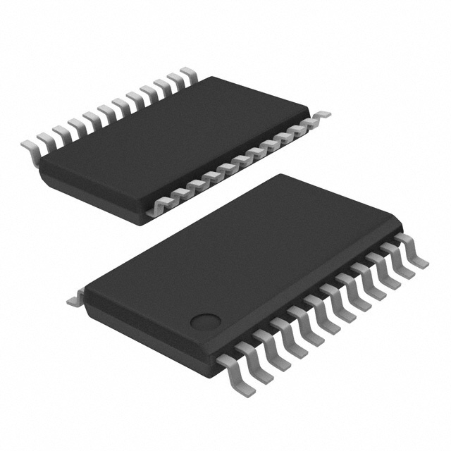
| Package Type | 24-TSSOP (0.173", 4.40mm Width) |
| Mounting Type | Surface Mount |
| PLL Function | Yes |
| Input Type | Clock |
| Output Type | Clock |
| Number of Circuits | 1 |
| Input:Output Ratio | 1:9 |
| Differential Input/Output | No/No |
| Maximum Frequency | 140MHz |
| Supply Voltage Range | 3V ~ 3.6V |
| Operating Temperature Range | 0°C ~ 85°C |
| RoHS Status | ROHS3 Compliant |
| Moisture Sensitivity Level | 1 (Unlimited) |
| Product Status | Obsolete |
Substitute Part Grouping Explanation
Substitute parts for the CDCF2509PW are identified based on the following critical parameters that determine functional compatibility:
Primary Substitution Criteria:
- Package type: 24-TSSOP form factor (identical mechanical footprint)
- Mounting type: Surface Mount
- PLL functionality: Present
- Supply voltage range: 3V ~ 3.6V (compatible with 3.3V systems)
- Operating temperature range: 0°C ~ 85°C
- Input/Output signal types: Clock-based signaling
- Single circuit configuration
- Non-differential input and output
Secondary Compatibility Factors:
- Maximum frequency rating (must meet or exceed application requirements)
- Input:Output ratio (determines clock multiplication/division capability)
- RoHS and MSL compliance status
The CDCVF2509APW qualifies as a direct substitute based on matching package, mounting type, voltage range, temperature range, and PLL architecture. Enhanced frequency capability (175MHz vs. 140MHz) provides additional operational margin for legacy system implementations.
Parameter Comparison
| Parameter | CDCF2509PW | CDCVF2509APW | Compatibility Notes |
|---|---|---|---|
| Manufacturer | Texas Instruments | Texas Instruments | Same manufacturer |
| Package Type | 24-TSSOP (0.173", 4.40mm Width) | 24-TSSOP (0.173", 4.40mm Width) | Identical footprint |
| Mounting Type | Surface Mount | Surface Mount | Compatible assembly process |
| PLL Function | Yes | Yes with Bypass | CDCVF2509APW includes bypass capability |
| Input Type | Clock | LVTTL | LVTTL is standard clock input signaling |
| Output Type | Clock | LVTTL | LVTTL is standard clock output signaling |
| Number of Circuits | 1 | 1 | Single circuit configuration |
| Input:Output Ratio | 1:9 | 2:10 | Different multiplication ratios; verify application requirement |
| Differential Input/Output | No/No | No/No | Both single-ended |
| Maximum Frequency | 140MHz | 175MHz | CDCVF2509APW rated higher; backward compatible |
| Supply Voltage Range | 3V ~ 3.6V | 3V ~ 3.6V | Identical voltage specification |
| Operating Temperature Range | 0°C ~ 85°C | 0°C ~ 85°C | Identical temperature specification |
| RoHS Status | ROHS3 Compliant | ROHS3 Compliant | Both compliant |
| Moisture Sensitivity Level | 1 (Unlimited) | 1 (Unlimited) | Identical MSL rating |
| Product Status | Obsolete | Obsolete | Both obsolete; sourcing from inventory stock |
Engineering Selection Recommendations
CDCVF2509APW as Primary Substitute:
The CDCVF2509APW is the manufacturer-recommended substitute for the CDCF2509PW. Both devices share identical package geometry (24-TSSOP), mounting type (Surface Mount), supply voltage range (3V ~ 3.6V), and operating temperature range (0°C ~ 85°C). Both maintain ROHS3 compliance and MSL Level 1 rating, ensuring equivalent handling and environmental performance.
The CDCVF2509APW provides a higher maximum frequency rating (175MHz vs. 140MHz), which ensures compatibility with applications originally designed for the CDCF2509PW while offering additional operational margin. The PLL with Bypass capability in the CDCVF2509APW provides enhanced flexibility compared to the standard PLL in the CDCF2509PW.
Critical Consideration - Input:Output Ratio:
The input:output ratio differs between the two devices (1:9 for CDCF2509PW vs. 2:10 for CDCVF2509APW). This parameter directly affects clock multiplication and must be verified against the specific application requirements. If the original design depends on the 1:9 ratio for timing synchronization or frequency generation, the 2:10 ratio of the substitute may require circuit-level validation.
Compliance and Sourcing:
Both devices are classified as obsolete products. Component selection should prioritize availability from verified inventory stock. Both devices maintain identical RoHS3 and REACH compliance status, supporting regulatory requirements for new designs and legacy system maintenance.
Frequently Asked Questions (FAQ)
Q: Can the CDCVF2509APW be used as a direct drop-in replacement for the CDCF2509PW?
A: The CDCVF2509APW is mechanically and electrically compatible in terms of package footprint, mounting type, pin count, supply voltage, and operating temperature range. However, the input:output ratio differs (2:10 vs. 1:9). Verify that your application does not depend on the specific 1:9 multiplication ratio before substitution.
Q: What is the significance of the different input:output ratios?
A: The input:output ratio determines the clock multiplication factor. The CDCF2509PW multiplies the input clock by 9, while the CDCVF2509APW multiplies by 10. If your circuit timing is dependent on a specific output frequency derived from a fixed input frequency, this difference must be evaluated.
Q: Are both devices available for new procurement?
A: Both the CDCF2509PW and CDCVF2509APW are classified as obsolete products. Component availability is limited to existing inventory stock. Current inventory levels are 1132 units for CDCF2509PW and 1287 units for CDCVF2509APW.
Q: Do the devices have identical environmental and compliance ratings?
A: Yes. Both devices are ROHS3 compliant, REACH unaffected, and rated at Moisture Sensitivity Level 1 (Unlimited). Both operate across the 0°C to 85°C temperature range and accept 3V to 3.6V supply voltage.
Q: What is the advantage of the CDCVF2509APW's higher frequency rating?
A: The CDCVF2509APW is rated to 175MHz compared to the CDCF2509PW's 140MHz. This higher rating provides operational margin and ensures the device can handle applications originally designed for the lower-rated part without frequency-related limitations.
Q: Are there any packaging or handling differences between these devices?
A: Both devices use the 24-TSSOP package with identical dimensions (0.173" width, 4.40mm). The CDCVF2509APW is supplied in Tube packaging. Both maintain MSL Level 1 rating, indicating unlimited shelf life under controlled storage conditions.
Alternative Parts

SJ6012L2TP
Littelfuse Inc.
6 Alternative Parts

JMK107BBJ476MA-RE
Taiyo Yuden
10 Alternative Parts

GMK107BBJ475MA-T
Taiyo Yuden
5 Alternative Parts
SJ6020N2ARP
Littelfuse Inc.
3 Alternative Parts
SJ6025R2ATP
Littelfuse Inc.
4 Alternative Parts

2474-05L
API Delevan Inc.
1 Alternative Parts

4590R-684K
API Delevan Inc.
1 Alternative Parts

CM6560R-334
API Delevan Inc.
1 Alternative Parts

CM6460-104
API Delevan Inc.
1 Alternative Parts

5526-12
API Delevan Inc.
1 Alternative Parts