


Request Quote
(Ships tomorrow)
CDCE925PWG4 Equivalent & Substitute Parts
Part Overview
The CDCE925PWG4 is a PLL Clock Generator IC manufactured by Texas Instruments, designed for applications requiring programmable clock generation up to 230MHz. This device features a single PLL circuit with bypass capability, accepting LVCMOS or Crystal inputs and delivering LVCMOS outputs with a 1:5 input-to-output ratio.
The CDCE925PWG4 is currently discontinued at DiGi Electronics. Identifying equivalent substitute parts is necessary to maintain design continuity and ensure component availability for production and replacement applications.
Substiute Parts
Key Parameters
| Parameter | Value |
|---|---|
| Manufacturer Part Number | CDCE925PWG4 |
| Manufacturer | Texas Instruments |
| Category | Clock/Timing |
| Type | PLL Clock Generator |
| Frequency - Max | 230MHz |
| Voltage - Supply | 1.7V ~ 1.9V |
| Operating Temperature | -40°C ~ 85°C |
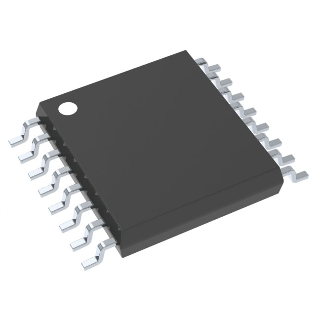
| Package / Case | 16-TSSOP (0.173", 4.40mm Width) |
| Mounting Type | Surface Mount |
| RoHS Status | ROHS3 Compliant |
| Moisture Sensitivity Level (MSL) | 1 (Unlimited) |
Substitute Part Grouping Explanation
Substitution of the CDCE925PWG4 is determined by the following critical parameters:
- Functional Type: PLL Clock Generator with bypass capability
- Maximum Frequency: 230MHz operation
- Supply Voltage Range: 1.7V ~ 1.9V
- Input/Output Signal Levels: LVCMOS and Crystal input compatibility; LVCMOS output
- Input-to-Output Ratio: 1:5
- Package Configuration: 16-TSSOP surface mount form factor
- Electrical Compliance: ROHS3 compliance and MSL Level 1 rating
Substitute parts must match all these parameters to ensure functional and physical compatibility within the original design.
Parameter Comparison
| Parameter | CDCE925PWG4 | CDCE925PW |
|---|---|---|
| Manufacturer Part Number | CDCE925PWG4 | CDCE925PW |
| Manufacturer | Texas Instruments | Texas Instruments |
| Type | PLL Clock Generator | PLL Clock Generator |
| PLL with Bypass | Yes | Yes |
| Input | LVCMOS, Crystal | LVCMOS, Crystal |
| Output | LVCMOS | LVCMOS |
| Number of Circuits | 1 | 1 |
| Ratio - Input:Output | 1:5 | 1:5 |
| Differential - Input:Output | No/No | No/No |
| Frequency - Max | 230MHz | 230MHz |
| Divider/Multiplier | Yes/No | Yes/No |
| Voltage - Supply | 1.7V ~ 1.9V | 1.7V ~ 1.9V |
| Operating Temperature | -40°C ~ 85°C | -40°C ~ 85°C |
| Mounting Type | Surface Mount | Surface Mount |
| Package / Case | 16-TSSOP (0.173", 4.40mm Width) | 16-TSSOP (0.173", 4.40mm Width) |
| RoHS Status | ROHS3 Compliant | ROHS3 Compliant |
| Moisture Sensitivity Level (MSL) | 1 (Unlimited) | 1 (Unlimited) |
| REACH Status | REACH Unaffected | REACH Unaffected |
| Product Status | Discontinued at DiGi Electronics | Active |
Engineering Selection Recommendations
The CDCE925PW is the direct substitute for the CDCE925PWG4. Both parts are manufactured by Texas Instruments and share identical electrical specifications, functional characteristics, and physical packaging. The primary distinction is product status: the CDCE925PWG4 is discontinued, while the CDCE925PW remains in active production.
Both parts maintain ROHS3 compliance and REACH unaffected status, meeting current regulatory requirements. The CDCE925PW is available in higher inventory quantities, supporting both new designs and replacement applications.
Frequently Asked Questions (FAQ)
Q: Can CDCE925PW directly replace CDCE925PWG4 in existing designs?
A: Yes. The CDCE925PW is electrically and mechanically identical to the CDCE925PWG4. All electrical parameters, signal characteristics, supply voltage requirements, operating temperature range, and package dimensions are equivalent. No design modifications are required.
Q: What is the difference between CDCE925PWG4 and CDCE925PW?
A: The primary difference is packaging and product status. CDCE925PWG4 is supplied in standard packaging and is discontinued. CDCE925PW is supplied in tube packaging and remains in active production. Electrical and functional specifications are identical.
Q: Are there any compliance or certification differences?
A: No. Both parts carry identical ROHS3 compliance, REACH unaffected status, and MSL Level 1 moisture sensitivity ratings. Both are suitable for applications with equivalent regulatory requirements.
Q: What is the 16-TSSOP package specification?
A: The 16-TSSOP (Thin Shrink Small Outline Package) is a surface mount package measuring 0.173 inches in height with a 4.40mm width. This package is standard for both the CDCE925PWG4 and CDCE925PW, ensuring identical PCB footprints and assembly compatibility.
Q: Can these parts operate at different supply voltages?
A: Both parts operate within the identical supply voltage range of 1.7V to 1.9V. No voltage adjustment or design modification is necessary when substituting between these parts.
Alternative Parts

SJ6012L2TP
Littelfuse Inc.
6 Alternative Parts

JMK107BBJ476MA-RE
Taiyo Yuden
10 Alternative Parts

GMK107BBJ475MA-T
Taiyo Yuden
5 Alternative Parts
SJ6020N2ARP
Littelfuse Inc.
3 Alternative Parts
SJ6025R2ATP
Littelfuse Inc.
4 Alternative Parts

2474-05L
API Delevan Inc.
1 Alternative Parts

4590R-684K
API Delevan Inc.
1 Alternative Parts

CM6560R-334
API Delevan Inc.
1 Alternative Parts

CM6460-104
API Delevan Inc.
1 Alternative Parts

5526-12
API Delevan Inc.
1 Alternative Parts