


Request Quote
(Ships tomorrow)
CDC706PW PLL Frequency Synthesizer Equivalent & Substitute Parts
Part Overview
The CDC706PW is a PLL Frequency Synthesizer IC manufactured by Texas Instruments, designed for clock and timing applications requiring frequency synthesis up to 300MHz. This device features a single PLL circuit with bypass capability, supporting both LVCMOS and Crystal inputs with LVCMOS output configuration.
The CDC706PW carries a "Not For New Designs" product status, indicating it has been superseded in Texas Instruments' product portfolio. Identifying equivalent substitute parts is necessary for ongoing production support, maintenance applications, and legacy system requirements where this component remains specified.
Substiute Parts
Key Parameters
| Parameter | Value |
|---|---|
| Manufacturer | Texas Instruments |
| Part Number | CDC706PW |
| Category | Clock/Timing - PLL Frequency Synthesizer |
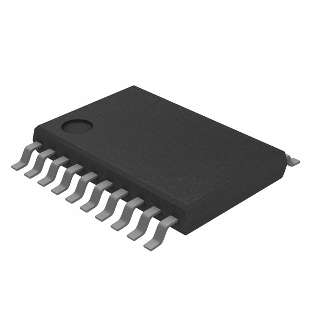
| Package Type | 20-TSSOP (0.173", 4.40mm Width) |
| Maximum Frequency | 300MHz |
| Input Type | LVCMOS, Crystal |
| Output Type | LVCMOS |
| Supply Voltage Range | 3V to 3.6V |
| Operating Temperature Range | -40°C to 85°C |
| Number of Circuits | 1 |
| Input:Output Ratio | 1:6 |
| PLL with Bypass | Yes |
| Mounting Type | Surface Mount |
| RoHS Status | ROHS3 Compliant |
| Moisture Sensitivity Level | 1 (Unlimited) |
Substitute Part Grouping Explanation
Substitution eligibility for the CDC706PW is determined by strict equivalence across the following critical parameters:
- Package and Pinout: 20-TSSOP form factor with identical pin configuration
- Electrical Specifications: Maximum frequency of 300MHz, supply voltage range 3V to 3.6V, operating temperature -40°C to 85°C
- Functional Architecture: Single PLL circuit with bypass capability
- Signal Interface: LVCMOS and Crystal input support with LVCMOS output
- Input:Output Ratio: 1:6 frequency division/multiplication ratio
- Compliance Standards: ROHS3 compliance and MSL Level 1 rating
The CDCE706PW qualifies as a parametric equivalent substitute based on complete alignment with all specified electrical, mechanical, and functional parameters.
Parameter Comparison
| Parameter | CDC706PW | CDCE706PW | Match |
|---|---|---|---|
| Manufacturer | Texas Instruments | Texas Instruments | ✓ |
| Package / Case | 20-TSSOP (0.173", 4.40mm Width) | 20-TSSOP (0.173", 4.40mm Width) | ✓ |
| Frequency - Max | 300MHz | 300MHz | ✓ |
| Input Type | LVCMOS, Crystal | LVCMOS, Crystal | ✓ |
| Output Type | LVCMOS | LVCMOS | ✓ |
| Voltage - Supply | 3V ~ 3.6V | 3V ~ 3.6V | ✓ |
| Operating Temperature | -40°C ~ 85°C | -40°C ~ 85°C | ✓ |
| Number of Circuits | 1 | 1 | ✓ |
| Ratio - Input:Output | 1:6 | 1:6 | ✓ |
| PLL with Bypass | Yes | Yes | ✓ |
| Mounting Type | Surface Mount | Surface Mount | ✓ |
| RoHS Status | ROHS3 Compliant | ROHS3 Compliant | ✓ |
| Moisture Sensitivity Level | 1 (Unlimited) | 1 (Unlimited) | ✓ |
| Product Status | Not For New Designs | Active | Upgrade Available |
Engineering Selection Recommendations
The CDCE706PW represents a direct parametric equivalent to the CDC706PW across all specified electrical, mechanical, and functional criteria. Both devices maintain identical performance characteristics within the 300MHz frequency range, supply voltage specifications, and operating temperature envelope.
The primary distinction lies in product lifecycle status: the CDC706PW is designated "Not For New Designs," while the CDCE706PW maintains "Active" product status from Texas Instruments. For applications requiring ongoing component availability and manufacturer support, the CDCE706PW is the preferred selection. Both parts maintain equivalent ROHS3 compliance and MSL Level 1 ratings, ensuring compatibility with standard manufacturing and storage protocols.
Frequently Asked Questions (FAQ)
Q: Can the CDCE706PW directly replace the CDC706PW in existing designs?
A: Yes. The CDCE706PW is a parametric equivalent with identical package, pinout, electrical specifications, and functional architecture. No circuit modifications are required for direct substitution.
Q: Are there any differences in supply voltage or operating temperature ranges?
A: No. Both parts operate across the identical 3V to 3.6V supply voltage range and -40°C to 85°C operating temperature range.
Q: Do both parts support the same input and output signal types?
A: Yes. Both the CDC706PW and CDCE706PW support LVCMOS and Crystal inputs with LVCMOS output configuration, maintaining the 1:6 input:output frequency ratio.
Q: What is the significance of the "Not For New Designs" status on the CDC706PW?
A: This designation indicates the CDC706PW has been superseded in Texas Instruments' product portfolio. While existing inventory remains available, the CDCE706PW is the recommended selection for new applications and ongoing production requirements.
Q: Are packaging and moisture sensitivity specifications identical?
A: Yes. Both parts are supplied in 20-TSSOP packages with MSL Level 1 (Unlimited) moisture sensitivity ratings, ensuring compatibility with standard surface mount assembly and storage conditions.
Q: What compliance certifications apply to both parts?
A: Both the CDC706PW and CDCE706PW maintain ROHS3 compliance and REACH Unaffected status, meeting current environmental and regulatory requirements.
Alternative Parts

SJ6012L2TP
Littelfuse Inc.
6 Alternative Parts

JMK107BBJ476MA-RE
Taiyo Yuden
10 Alternative Parts

GMK107BBJ475MA-T
Taiyo Yuden
5 Alternative Parts
SJ6020N2ARP
Littelfuse Inc.
3 Alternative Parts
SJ6025R2ATP
Littelfuse Inc.
4 Alternative Parts

2474-05L
API Delevan Inc.
1 Alternative Parts

4590R-684K
API Delevan Inc.
1 Alternative Parts

CM6560R-334
API Delevan Inc.
1 Alternative Parts

CM6460-104
API Delevan Inc.
1 Alternative Parts

5526-12
API Delevan Inc.
1 Alternative Parts