


Request Quote
(Ships tomorrow)
CDC5806PW Equivalent & Substitute Parts
Part Overview
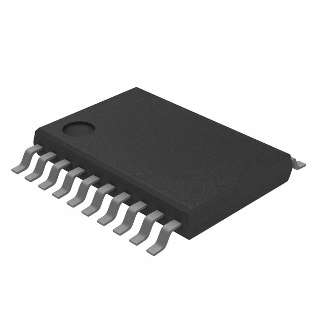
The CDC5806PW is a PLL Clock Generator IC manufactured by Texas Instruments, designed for clock generation applications requiring up to 74MHz output frequency. This device features a 1:6 input-to-output ratio with LVCMOS and LVTTL signal compatibility in a 20-TSSOP surface mount package.
The CDC5806PW is classified as obsolete. Identifying suitable substitute components is necessary to maintain design continuity and ensure component availability for new production runs or system updates.
Substiute Parts
Key Parameters
| Parameter | Value |
|---|---|
| Manufacturer Part Number | CDC5806PW |
| Manufacturer | Texas Instruments |
| Category | Clock/Timing |
| Type | PLL Clock Generator |
| Frequency - Max | 74MHz |
| Voltage - Supply | 3V ~ 3.6V |
| Package / Case | 20-TSSOP (0.173", 4.40mm Width) |
| Operating Temperature | -40°C ~ 85°C |
| Product Status | Obsolete |
| RoHS Status | ROHS3 Compliant |
Substitute Part Grouping Explanation
Substitution of the CDC5806PW is based on the following critical parameters:
- Package Compatibility: Both devices must use the 20-TSSOP (0.173", 4.40mm Width) surface mount package to ensure PCB layout compatibility without redesign.
- Supply Voltage: Operating voltage range must be 3V ~ 3.6V to match the original design specifications.
- Signal Compatibility: Input and output signal types (LVCMOS, LVTTL) must be compatible with existing circuit interfaces.
- Functional Capability: The substitute must provide PLL-based clock generation with bypass capability.
- Ratio Configuration: Input-to-output ratio of 1:6 must be supported or achievable through device configuration.
The CDCE906PW meets these substitution criteria while offering enhanced specifications and active product status.
Parameter Comparison
| Parameter | CDC5806PW (Original) | CDCE906PW (Substitute) |
|---|---|---|
| Manufacturer | Texas Instruments | Texas Instruments |
| Type | PLL Clock Generator | PLL Frequency Synthesizer |
| PLL with Bypass | Yes | Yes |
| Input Signal Types | LVCMOS, LVTTL | LVCMOS, Crystal |
| Output Signal Types | LVCMOS, LVTTL | LVCMOS |
| Number of Circuits | 1 | 1 |
| Ratio - Input:Output | 1:6 | 1:6 |
| Frequency - Max | 74MHz | 167MHz |
| Divider/Multiplier | Yes/No | Yes/Yes |
| Voltage - Supply | 3V ~ 3.6V | 3V ~ 3.6V |
| Operating Temperature | -40°C ~ 85°C | 0°C ~ 70°C |
| Package / Case | 20-TSSOP (0.173", 4.40mm Width) | 20-TSSOP (0.173", 4.40mm Width) |
| Mounting Type | Surface Mount | Surface Mount |
| Product Status | Obsolete | Active |
| RoHS Status | ROHS3 Compliant | ROHS3 Compliant |
| MSL Rating | 1 (Unlimited) | 1 (Unlimited) |
Engineering Selection Recommendations
The CDCE906PW is a direct substitute for the CDC5806PW based on the following factors:
- Package Equivalence: Identical 20-TSSOP package ensures no PCB layout modifications are required.
- Supply Voltage Compatibility: Both devices operate within the 3V ~ 3.6V range, maintaining power supply compatibility.
- Functional Compatibility: Both devices provide PLL-based clock generation with bypass capability and support the required 1:6 input-to-output ratio.
- Regulatory Compliance: The CDCE906PW maintains ROHS3 compliance and identical MSL rating, ensuring manufacturing and environmental standards alignment.
- Active Product Status: The CDCE906PW is an active product with verified programmability, providing long-term availability and supply chain stability compared to the obsolete CDC5806PW.
Temperature range differences should be evaluated against specific application requirements. The CDCE906PW operates from 0°C ~ 70°C, which is narrower than the original CDC5806PW range of -40°C ~ 85°C. Applications requiring extended temperature operation below 0°C or above 70°C must verify compatibility with the substitute device specifications.
Frequently Asked Questions (FAQ)
Q: Can the CDCE906PW directly replace the CDC5806PW without PCB modifications?
A: Yes. Both devices use the identical 20-TSSOP package with matching pinout compatibility for clock generation applications. No PCB layout changes are required for package substitution.
Q: What are the key differences between these devices?
A: The CDCE906PW is a PLL Frequency Synthesizer offering higher maximum frequency (167MHz vs. 74MHz) and includes multiplier capability in addition to divider functions. The CDCE906PW supports crystal input in addition to LVCMOS, while output is limited to LVCMOS. Operating temperature range is narrower (0°C ~ 70°C vs. -40°C ~ 85°C).
Q: Are there any signal compatibility concerns?
A: The CDC5806PW supports both LVCMOS and LVTTL output signals. The CDCE906PW provides LVCMOS output only. Designs requiring LVTTL output must verify that LVCMOS levels are acceptable for downstream logic interfaces.
Q: Does the CDCE906PW support the same input-to-output ratio?
A: Yes. Both devices support a 1:6 input-to-output ratio configuration. The CDCE906PW provides additional flexibility through multiplier capability for alternative ratio configurations if required.
Q: What is the impact of the narrower operating temperature range?
A: The CDCE906PW operates from 0°C ~ 70°C, compared to the CDC5806PW range of -40°C ~ 85°C. Applications operating below 0°C or above 70°C must confirm that the substitute device meets temperature requirements before implementation.
Q: Are compliance certifications equivalent?
A: Yes. Both devices are ROHS3 compliant with identical MSL rating of 1 (Unlimited), ensuring equivalent environmental and manufacturing compliance standards.
Alternative Parts

SJ6012L2TP
Littelfuse Inc.
6 Alternative Parts

JMK107BBJ476MA-RE
Taiyo Yuden
10 Alternative Parts

GMK107BBJ475MA-T
Taiyo Yuden
5 Alternative Parts
SJ6020N2ARP
Littelfuse Inc.
3 Alternative Parts
SJ6025R2ATP
Littelfuse Inc.
4 Alternative Parts

2474-05L
API Delevan Inc.
1 Alternative Parts

4590R-684K
API Delevan Inc.
1 Alternative Parts

CM6560R-334
API Delevan Inc.
1 Alternative Parts

CM6460-104
API Delevan Inc.
1 Alternative Parts

5526-12
API Delevan Inc.
1 Alternative Parts