


Request Quote
(Ships tomorrow)
CD4503BCN Equivalent & Substitute Parts
Part Overview
The CD4503BCN is a non-inverting buffer IC from the 4000B logic series, designed for digital signal buffering applications. This device features 2 elements with 2 and 4 (Hex) bit configurations per element, delivering push-pull output capability across a wide supply voltage range of 3V to 15V. The CD4503BCN is classified as obsolete, making identification of functionally equivalent substitute parts essential for ongoing system maintenance, repair, and legacy product support.
Substiute Parts
Key Parameters
| Parameter | Value |
|---|---|
| Manufacturer Part Number | CD4503BCN |
| Manufacturer | onsemi |
| Logic Type | Buffer, Non-Inverting |
| Number of Elements | 2 |
| Number of Bits per Element | 2, 4 (Hex) |
| Output Type | Push-Pull |
| Current - Output High, Low | 17.6mA, 25mA |
| Voltage - Supply | 3V ~ 15V |
| Operating Temperature | -55°C ~ 125°C (TA) |
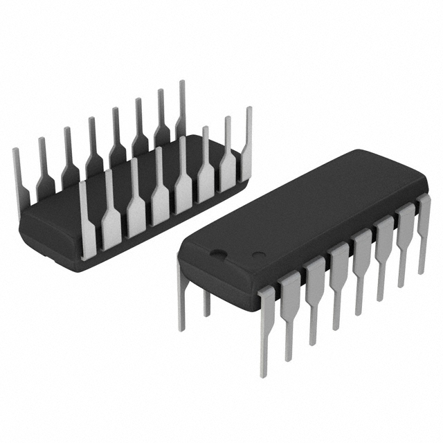
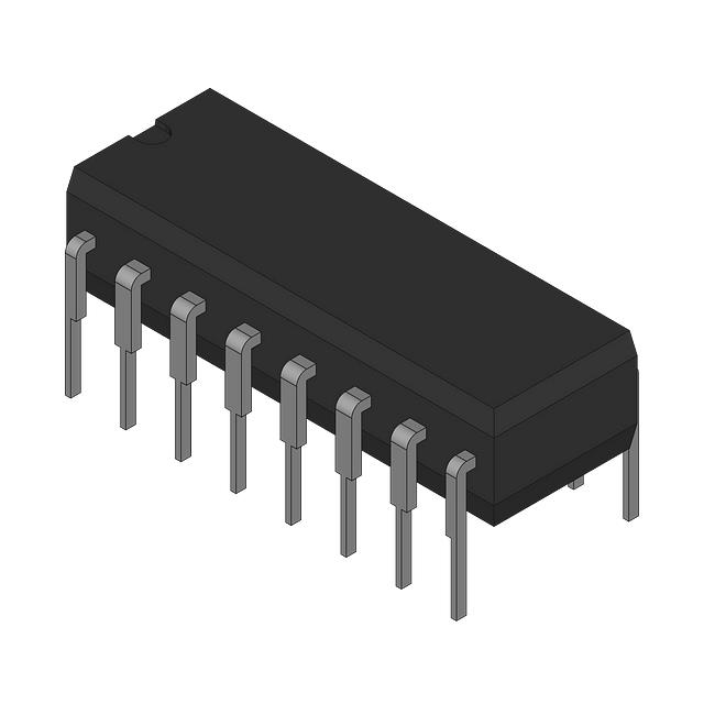
| Package / Case | 16-DIP (0.300", 7.62mm) |
| Mounting Type | Through Hole |
| Series | 4000B |
| Product Status | Obsolete |
Substitute Part Grouping Explanation
Substitution of the CD4503BCN is determined by strict alignment of the following critical parameters:
- Logic Function: Buffer, Non-Inverting configuration with identical element and bit-per-element architecture (2 elements, 2 and 4 Hex bits)
- Output Characteristics: Push-Pull output type with compatible current ratings
- Supply Voltage Range: Minimum 3V operation; maximum supply voltage must equal or exceed 15V
- Package Compatibility: 16-DIP (0.300", 7.62mm) through-hole mounting
- Operating Temperature Range: -55°C to 125°C (TA)
- Series Classification: 4000B logic family
The CD4503BE qualifies as a direct substitute based on these parameters. Both devices share identical logic architecture, package form factor, and thermal operating range. The CD4503BE extends the maximum supply voltage to 18V, providing enhanced voltage margin while maintaining full backward compatibility with CD4503BCN applications.
Parameter Comparison
| Parameter | CD4503BCN (Main) | CD4503BE (Substitute) |
|---|---|---|
| Manufacturer | onsemi | Harris Corporation |
| Logic Type | Buffer, Non-Inverting | Buffer, Non-Inverting |
| Number of Elements | 2 | 2 |
| Number of Bits per Element | 2, 4 (Hex) | 2, 4 (Hex) |
| Output Type | Push-Pull | Push-Pull |
| Current - Output High, Low | 17.6mA, 25mA | 14.1mA, 23mA |
| Voltage - Supply | 3V ~ 15V | 3V ~ 18V |
| Operating Temperature | -55°C ~ 125°C (TA) | -55°C ~ 125°C (TA) |
| Package / Case | 16-DIP (0.300", 7.62mm) | 16-DIP (0.300", 7.62mm) |
| Mounting Type | Through Hole | Through Hole |
| Series | 4000B | 4000B |
| Product Status | Obsolete | Obsolete |
Engineering Selection Recommendations
Both the CD4503BCN and CD4503BE are classified as obsolete products. Selection between these devices should be based on the following engineering criteria:
CD4503BCN (onsemi): Select this part when legacy documentation or design specifications explicitly reference the onsemi manufacturer variant and when supply voltage is constrained to 15V maximum.
CD4503BE (Harris Corporation): This substitute provides extended supply voltage capability (18V maximum) while maintaining identical logic function and package compatibility. The CD4503BE is suitable for applications requiring voltage margin above 15V or when onsemi sourcing is unavailable. Output current specifications are slightly lower (14.1mA high, 23mA low versus 17.6mA high, 25mA low), which is acceptable for standard buffering applications within the 4000B logic family.
Both devices operate across the full -55°C to 125°C temperature range and are housed in identical 16-DIP through-hole packages, ensuring direct mechanical and electrical interchangeability in PCB designs.
Frequently Asked Questions (FAQ)
Q: Can the CD4503BE directly replace the CD4503BCN in existing designs?
A: Yes. Both devices share identical logic architecture (2-element, 2/4-bit non-inverting buffer), package form factor (16-DIP), and operating temperature range (-55°C to 125°C). The CD4503BE is electrically and mechanically compatible with the CD4503BCN.
Q: What is the key difference between these two parts?
A: The primary difference is maximum supply voltage. The CD4503BCN operates from 3V to 15V, while the CD4503BE extends to 18V. Output current ratings are also slightly different: CD4503BCN delivers 17.6mA (high) and 25mA (low), compared to CD4503BE at 14.1mA (high) and 23mA (low).
Q: Are there any compliance or RoHS considerations?
A: The CD4503BE is marked as RoHS non-compliant. If RoHS compliance is required for your application, verify that the CD4503BCN meets your compliance requirements before selection.
Q: Why are both parts classified as obsolete?
A: Both the CD4503BCN and CD4503BE are legacy 4000B series logic devices. Modern designs typically use contemporary CMOS logic families. However, these parts remain available through authorized distributors for repair, maintenance, and legacy system support.
Q: Can I use the CD4503BE in a circuit designed for 15V maximum supply?
A: Yes. The CD4503BE operates across 3V to 18V, which includes the 3V to 15V range of the CD4503BCN. The extended voltage rating does not affect operation within the lower voltage range.
Q: Are the pin configurations identical?
A: Yes. Both devices use the 16-DIP (0.300", 7.62mm) through-hole package with identical pinout, enabling direct PCB substitution without layout modifications.
Alternative Parts

SJ6012L2TP
Littelfuse Inc.
6 Alternative Parts

JMK107BBJ476MA-RE
Taiyo Yuden
10 Alternative Parts

GMK107BBJ475MA-T
Taiyo Yuden
5 Alternative Parts
SJ6020N2ARP
Littelfuse Inc.
3 Alternative Parts
SJ6025R2ATP
Littelfuse Inc.
4 Alternative Parts

2474-05L
API Delevan Inc.
1 Alternative Parts

4590R-684K
API Delevan Inc.
1 Alternative Parts

CM6560R-334
API Delevan Inc.
1 Alternative Parts

CM6460-104
API Delevan Inc.
1 Alternative Parts

5526-12
API Delevan Inc.
1 Alternative Parts