


Request Quote
(Ships tomorrow)
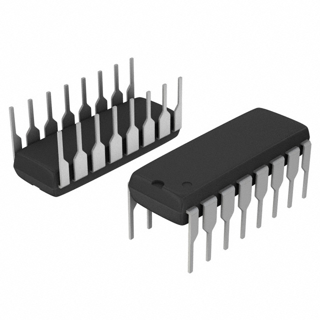
CD4050BCN Equivalent & Substitute Parts
Part Overview
The CD4050BCN is a non-inverting buffer IC from onsemi's 4000B logic series, designed for signal buffering applications requiring 6 independent buffer elements with push-pull output capability. This device operates across a wide supply voltage range of 3V to 15V and supports operating temperatures from -55°C to 125°C. The CD4050BCN is classified as obsolete, making equivalent and substitute parts necessary for ongoing system maintenance, repairs, and legacy design support.
Substiute Parts
Key Parameters
| Parameter | Value |
|---|---|
| Manufacturer Part Number | CD4050BCN |
| Manufacturer | onsemi |
| Logic Type | Buffer, Non-Inverting |
| Number of Elements | 6 |
| Number of Bits per Element | 1 |
| Output Type | Push-Pull |
| Current - Output High, Low | 12mA, 40mA |
| Voltage - Supply | 3V ~ 15V |
| Operating Temperature | -55°C ~ 125°C (TA) |
| Package / Case | 16-DIP (0.300", 7.62mm) |
| Mounting Type | Through Hole |
| Product Status | Obsolete |
Substitute Part Grouping Explanation
Substitution eligibility for the CD4050BCN is determined by the following critical parameters:
- Logic Function: Must be a non-inverting buffer with 6 independent elements
- Output Configuration: Push-pull output topology required
- Package Type: 16-DIP through-hole package (0.300", 7.62mm) for mechanical compatibility
- Supply Voltage Range: Must support operation within or encompass the 3V to 15V range
- Output Current Ratings: Must meet or exceed the specified output current capabilities (12mA high, 40mA low)
- Operating Temperature Range: Must support -55°C to 125°C operation
- Base Product Series: 4000B logic family
The CD4050BE qualifies as a direct substitute based on these parameters. Both devices share identical logic architecture, element count, output type, package configuration, and thermal operating range. The CD4050BE extends the maximum supply voltage to 18V, providing enhanced voltage margin while maintaining full backward compatibility with CD4050BCN applications.
Parameter Comparison
| Parameter | CD4050BCN (onsemi) | CD4050BE (Harris Corporation) |
|---|---|---|
| Logic Type | Buffer, Non-Inverting | Buffer, Non-Inverting |
| Number of Elements | 6 | 6 |
| Number of Bits per Element | 1 | 1 |
| Output Type | Push-Pull | Push-Pull |
| Current - Output High, Low | 12mA, 40mA | 8mA, 48mA |
| Voltage - Supply | 3V ~ 15V | 3V ~ 18V |
| Operating Temperature | -55°C ~ 125°C (TA) | -55°C ~ 125°C (TA) |
| Package / Case | 16-DIP (0.300", 7.62mm) | 16-DIP (0.300", 7.62mm) |
| Mounting Type | Through Hole | Through Hole |
| Base Product Series | 4000B | 4000B |
| Product Status | Obsolete | Obsolete |
Engineering Selection Recommendations
Both the CD4050BCN and CD4050BE are classified as obsolete products. The CD4050BE serves as a functional equivalent with the following considerations:
Voltage Compatibility: The CD4050BE supports supply voltages up to 18V compared to the CD4050BCN's 15V maximum. Applications operating at or below 15V will experience full compatibility. Systems designed for the extended 15V to 18V range benefit from the CD4050BE's enhanced voltage margin.
Output Current Characteristics: The CD4050BE delivers 8mA output high current (versus 12mA) and 48mA output low current (versus 40mA). Circuit designs must confirm that the reduced high-side current does not impact signal integrity or load requirements, while the increased low-side current provides additional drive capability.
RoHS Compliance Status: The CD4050BCN status is unspecified in available documentation. The CD4050BE is documented as RoHS non-compliant. Applications subject to RoHS requirements must address this compliance gap through alternative sourcing or design modification.
Packaging and Mounting: Both devices utilize identical 16-DIP through-hole packages, ensuring direct mechanical and electrical pin compatibility on existing PCB layouts.
Frequently Asked Questions (FAQ)
Q: Can the CD4050BE directly replace the CD4050BCN in existing designs?
A: Yes, for applications operating at supply voltages of 15V or below. The CD4050BE is pin-compatible and functionally equivalent. Designs utilizing the full 15V supply voltage will operate within the CD4050BE's specified range. Output current differences must be evaluated against specific load requirements.
Q: What is the impact of the different output current ratings?
A: The CD4050BE provides lower output high current (8mA vs. 12mA) but higher output low current (48mA vs. 40mA). Applications driving capacitive loads or requiring high source current may be affected by the reduced high-side drive. Applications requiring high sink current benefit from the increased low-side capability.
Q: Are there package compatibility concerns?
A: No. Both the CD4050BCN and CD4050BE use identical 16-DIP through-hole packages with 0.300" (7.62mm) row spacing. Direct socket substitution is mechanically and electrically feasible.
Q: What is the significance of the extended voltage range in the CD4050BE?
A: The CD4050BE supports operation up to 18V supply voltage, compared to the CD4050BCN's 15V maximum. This provides additional design margin for systems operating near the upper voltage limit and accommodates applications requiring higher supply voltages.
Q: How should RoHS compliance be addressed when substituting parts?
A: Both devices are obsolete and documented as RoHS non-compliant or unspecified. Applications subject to RoHS requirements must evaluate alternative modern buffer IC solutions or confirm exemption status for legacy system maintenance.
Q: Are there thermal or operating temperature differences?
A: No. Both devices operate identically across the -55°C to 125°C temperature range, ensuring equivalent thermal performance in all operating environments.
Alternative Parts

SJ6012L2TP
Littelfuse Inc.
6 Alternative Parts

JMK107BBJ476MA-RE
Taiyo Yuden
10 Alternative Parts

GMK107BBJ475MA-T
Taiyo Yuden
5 Alternative Parts
SJ6020N2ARP
Littelfuse Inc.
3 Alternative Parts
SJ6025R2ATP
Littelfuse Inc.
4 Alternative Parts

2474-05L
API Delevan Inc.
1 Alternative Parts

4590R-684K
API Delevan Inc.
1 Alternative Parts

CM6560R-334
API Delevan Inc.
1 Alternative Parts

CM6460-104
API Delevan Inc.
1 Alternative Parts

5526-12
API Delevan Inc.
1 Alternative Parts