


Request Quote
(Ships tomorrow)
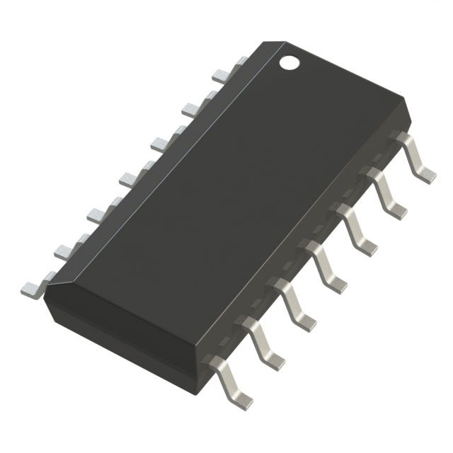
CD4013BCSJ Equivalent & Substitute Parts
Part Overview
The CD4013BCSJ is a dual D-type flip-flop logic integrated circuit manufactured by onsemi in the 4000B CMOS series. This device features complementary outputs, positive edge triggering, and operates across a wide supply voltage range of 3V to 15V. The part is currently classified as obsolete, making identification of functionally equivalent alternatives essential for design continuity and procurement planning. Substitute parts must maintain functional compatibility while meeting the electrical and mechanical requirements of the original specification.
Substiute Parts
Key Parameters
| Parameter | CD4013BCSJ |
|---|---|
| Manufacturer | onsemi |
| Product Status | Obsolete |
| Type | D-Type Flip Flop, 2 Element, 1 Bit |
| Output Type | Complementary |
| Clock Frequency | 15.5 MHz |
| Max Propagation Delay @ 15V, 50pF | 120 ns |
| Voltage Supply Range | 3V ~ 15V |
| Current Output High/Low | 8.8 mA / 8.8 mA |
| Quiescent Current (Iq) | 4 µA |
| Operating Temperature | -55°C ~ 125°C |
| Package | 14-SOIC (0.209", 5.30mm Width) |
| Mounting Type | Surface Mount |
| Series | 4000B |
Substitute Part Grouping Explanation
Substitute parts for the CD4013BCSJ are qualified based on the following criteria:
Functional Equivalence: All substitute parts must be dual D-type flip-flops with complementary outputs, positive edge triggering, and 2 elements of 1 bit each.
Electrical Compatibility: Substitute parts must support the supply voltage range of 3V to 15V and maintain compatible quiescent current specifications (4 µA).
Mechanical Compatibility: All substitute parts must use the 14-SOIC surface mount package with compatible pinout and footprint dimensions.
Performance Parameters: Clock frequency, propagation delay, and output current specifications may vary within acceptable ranges for logic circuit applications, provided the substitute meets or exceeds the minimum performance requirements of the original part.
Compliance & Status: Active product status and RoHS compliance are preferred for new designs, though obsolete status does not disqualify a substitute if all electrical and mechanical parameters align.
Parameter Comparison
| Parameter | CD4013BCSJ (onsemi) | CD4013BNSR (Texas Instruments) | HEF4013BT,653 (Nexperia USA Inc.) |
|---|---|---|---|
| Product Status | Obsolete | Active | Active |
| Type | D-Type Flip Flop, 2 Element, 1 Bit | D-Type Flip Flop, 2 Element, 1 Bit | D-Type Flip Flop, 2 Element, 1 Bit |
| Output Type | Complementary | Complementary | Complementary |
| Clock Frequency | 15.5 MHz | 24 MHz | 40 MHz |
| Max Propagation Delay @ 15V, 50pF | 120 ns | 90 ns | 60 ns |
| Voltage Supply Range | 3V ~ 15V | 3V ~ 18V | 3V ~ 15V |
| Current Output High/Low | 8.8 mA / 8.8 mA | 6.8 mA / 6.8 mA | 3.4 mA / 3.4 mA |
| Quiescent Current (Iq) | 4 µA | 4 µA | 4 µA |
| Input Capacitance | 5 pF | 5 pF | 7.5 pF |
| Operating Temperature | -55°C ~ 125°C | -55°C ~ 125°C | -40°C ~ 125°C |
| Package | 14-SOIC (0.209", 5.30mm Width) | 14-SOIC (0.209", 5.30mm Width) | 14-SOIC (0.154", 3.90mm Width) |
| Series | 4000B | 4000B | 4000B |
| RoHS Status | Not specified | ROHS3 Compliant | ROHS3 Compliant |
Engineering Selection Recommendations
CD4013BNSR (Texas Instruments): This part is functionally equivalent to the CD4013BCSJ with active product status and ROHS3 compliance. It maintains the same 14-SOIC package footprint (0.209", 5.30mm Width), identical quiescent current, and compatible supply voltage range. The CD4013BNSR offers improved performance with 24 MHz clock frequency and 90 ns propagation delay, making it suitable for direct substitution in new designs and legacy system replacements.
HEF4013BT,653 (Nexperia USA Inc.): This part provides the highest performance specification within the 4000B series with 40 MHz clock frequency and 60 ns propagation delay. It maintains ROHS3 compliance and active product status. The HEF4013BT,653 uses a narrower 14-SOIC package (0.154", 3.90mm Width), which requires PCB layout verification before implementation. The reduced output current (3.4 mA) and extended input capacitance (7.5 pF) must be evaluated against circuit load requirements. This part is suitable for applications requiring enhanced speed performance and space-constrained designs.
Frequently Asked Questions (FAQ)
Q: Can the CD4013BNSR directly replace the CD4013BCSJ on existing PCBs?
A: Yes. Both parts use the same 14-SOIC package footprint (0.209", 5.30mm Width) and pinout. The CD4013BNSR maintains electrical compatibility across the 3V to 15V supply range and identical quiescent current specifications. No circuit modifications are required.
Q: Is the HEF4013BT,653 compatible with the original CD4013BCSJ design?
A: Electrical compatibility is maintained; however, the HEF4013BT,653 uses a narrower 14-SOIC package (0.154", 3.90mm Width) compared to the CD4013BCSJ (0.209", 5.30mm Width). PCB footprint verification is required before substitution. The reduced output current and increased input capacitance must be evaluated for circuit load compatibility.
Q: What are the key differences between the substitute parts?
A: The CD4013BNSR offers moderate performance improvement (24 MHz, 90 ns delay) with identical package dimensions. The HEF4013BT,653 provides superior performance (40 MHz, 60 ns delay) with a narrower package and lower output current. Selection depends on performance requirements, PCB layout constraints, and load specifications.
Q: Are all substitute parts RoHS compliant?
A: The CD4013BNSR and HEF4013BT,653 are both ROHS3 compliant. The original CD4013BCSJ RoHS status is not specified in the available documentation.
Q: What is the operating temperature range for each part?
A: The CD4013BCSJ and CD4013BNSR operate from -55°C to 125°C. The HEF4013BT,653 operates from -40°C to 125°C. For applications requiring the full -55°C lower temperature limit, the CD4013BNSR is the appropriate choice.
Alternative Parts

SJ6012L2TP
Littelfuse Inc.
6 Alternative Parts

JMK107BBJ476MA-RE
Taiyo Yuden
10 Alternative Parts

GMK107BBJ475MA-T
Taiyo Yuden
5 Alternative Parts
SJ6020N2ARP
Littelfuse Inc.
3 Alternative Parts
SJ6025R2ATP
Littelfuse Inc.
4 Alternative Parts

2474-05L
API Delevan Inc.
1 Alternative Parts

4590R-684K
API Delevan Inc.
1 Alternative Parts

CM6560R-334
API Delevan Inc.
1 Alternative Parts

CM6460-104
API Delevan Inc.
1 Alternative Parts

5526-12
API Delevan Inc.
1 Alternative Parts