


Request Quote
(Ships tomorrow)
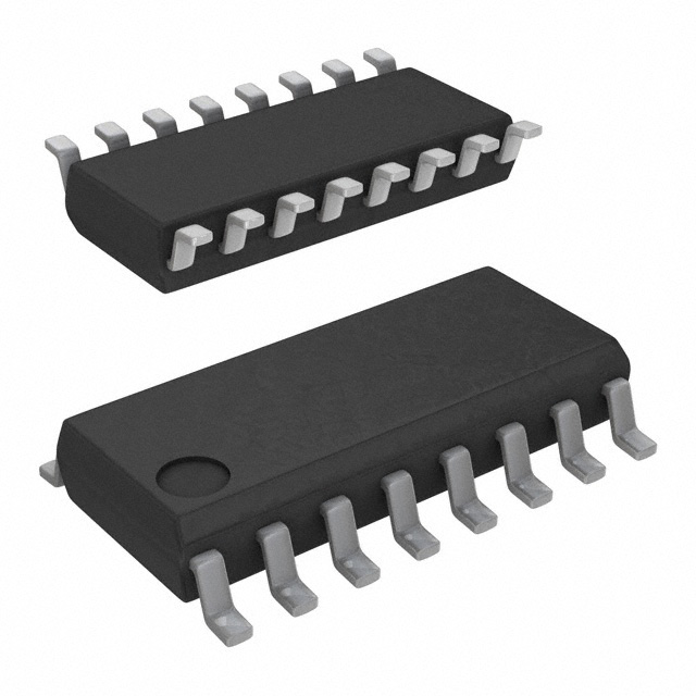
C8051F803-GS Equivalent & Substitute Parts
Part Overview
The C8051F803-GS is an 8-bit microcontroller from Silicon Labs' C8051F80x series, featuring a 25MHz 8051 core with 16KB FLASH memory and integrated peripherals including SMBus, SPI, UART, and capacitive sensing capabilities. This device is classified as Last Time Buy, indicating end-of-life status. Identifying equivalent and substitute parts is necessary to ensure design continuity and support for new production runs or long-term system maintenance.
Substiute Parts
Key Parameters
| Parameter | Value |
|---|---|
| Core Processor Architecture | 8-Bit |
| Program Memory | 16KB FLASH |
| Operating Speed | 25MHz |
| Supply Voltage Range | 1.8V ~ 3.6V |
| Operating Temperature | -40°C ~ 85°C |
| Package Type | 16-SOIC |
| I/O Count | 13 |
| Data Converters | A/D 12x10b |
| Connectivity Interfaces | SMBus (2-Wire/I2C), SPI, UART/USART |
| RoHS Compliance | RoHS Compliant |
Substitute Part Grouping Explanation
The ATTINY167-SU from Microchip Technology is identified as a substitute based on the following alignment criteria:
Matching Parameters:
- 8-Bit core processor architecture
- 16KB program FLASH memory capacity
- Identical operating temperature range (-40°C ~ 85°C)
- Surface mount technology (SOIC package family)
- Internal oscillator configuration
- Integrated peripherals: PWM, WDT, Temperature Sensor, Power-On Reset
- Common communication interfaces: I2C, SPI, UART/USART
- RoHS and REACH compliance
Differing Parameters:
- Operating speed: 16MHz (ATTINY167-SU) vs. 25MHz (C8051F803-GS)
- Package footprint: 20-SOIC vs. 16-SOIC
- I/O pin count: 16 vs. 13
- Supply voltage range: 1.8V ~ 5.5V vs. 1.8V ~ 3.6V
- A/D converter resolution: 11x10b vs. 12x10b
- Processor core: AVR vs. 8051
Parameter Comparison
| Parameter | C8051F803-GS | ATTINY167-SU | Compatibility Notes |
|---|---|---|---|
| Core Size | 8-Bit | 8-Bit | Matched |
| Program Memory | 16KB FLASH | 16KB FLASH | Matched |
| Operating Speed | 25MHz | 16MHz | ATTINY167-SU operates at lower frequency |
| Supply Voltage | 1.8V ~ 3.6V | 1.8V ~ 5.5V | ATTINY167-SU supports wider range |
| Operating Temperature | -40°C ~ 85°C | -40°C ~ 85°C | Matched |
| Package Type | 16-SOIC | 20-SOIC | Different footprint; PCB layout modification required |
| I/O Pins | 13 | 16 | ATTINY167-SU provides additional I/O |
| A/D Converter | 12x10b | 11x10b | C8051F803-GS has higher resolution |
| Communication Interfaces | SMBus, SPI, UART | I2C, SPI, UART, USI, LINbus | Both support core interfaces; ATTINY167-SU adds LINbus and USI |
| RoHS Status | RoHS Compliant | ROHS3 Compliant | Both compliant; ATTINY167-SU meets latest standard |
| Product Status | Last Time Buy | Active | ATTINY167-SU actively manufactured |
Engineering Selection Recommendations
Selection between the C8051F803-GS and ATTINY167-SU depends on application-specific requirements:
Choose ATTINY167-SU when:
- Design can accommodate 20-SOIC package footprint or PCB redesign is feasible
- 16MHz operating speed meets application timing requirements
- Extended supply voltage range (up to 5.5V) is beneficial
- Additional I/O pins (16 vs. 13) provide design flexibility
- LINbus or USI interface support is required
- Active product availability and long-term supply assurance are priorities
- ROHS3 compliance is mandated
Retain C8051F803-GS when:
- 25MHz speed is critical for application performance
- 16-SOIC package footprint is fixed in existing PCB design
- 12-bit A/D converter resolution is required
- SMBus interface is specifically required
- Existing firmware is optimized for 8051 architecture
- Supply voltage must remain below 3.6V
Both devices maintain identical operating temperature range and core memory capacity, supporting functional equivalence in many embedded applications. However, architectural differences (8051 vs. AVR), package form factor, and performance specifications require detailed application analysis before substitution.
Frequently Asked Questions (FAQ)
Q: Can ATTINY167-SU directly replace C8051F803-GS without PCB modification?
A: No. The ATTINY167-SU uses a 20-SOIC package versus the 16-SOIC package of the C8051F803-GS. PCB layout redesign is required. Additionally, the different processor architecture (AVR vs. 8051) necessitates firmware recompilation or rewriting.
Q: What is the primary limitation of ATTINY167-SU as a substitute?
A: Operating speed is reduced from 25MHz to 16MHz. Applications with strict timing requirements or high-frequency signal processing may not be compatible. Verify that 16MHz operation satisfies all timing-critical functions in your design.
Q: Are the communication interfaces compatible?
A: Both devices support I2C, SPI, and UART/USART interfaces. The C8051F803-GS specifically implements SMBus (2-Wire), while the ATTINY167-SU implements I2C and includes additional interfaces (LINbus, USI). For SMBus-specific requirements, verify I2C compatibility in your application protocol.
Q: What are the memory differences?
A: Both devices provide 16KB FLASH program memory and 512 x 8 RAM. The C8051F803-GS includes a 12-bit A/D converter (12x10b), while the ATTINY167-SU provides an 11-bit A/D converter (11x10b). For applications requiring 12-bit resolution, the C8051F803-GS is preferred.
Q: Is firmware migration required?
A: Yes. The C8051F803-GS uses the 8051 instruction set, while the ATTINY167-SU uses the AVR instruction set. Complete firmware recompilation or rewriting is necessary. Development tools, compiler support, and debugging infrastructure differ between architectures.
Q: Which device has better long-term availability?
A: The ATTINY167-SU is classified as Active product status with 1134 units in stock, ensuring ongoing manufacturing and supply. The C8051F803-GS is Last Time Buy, indicating end-of-life status with limited future availability.
Q: Can I use ATTINY167-SU in a 3.3V system?
A: Yes. The ATTINY167-SU supply voltage range (1.8V ~ 5.5V) encompasses 3.3V operation. The C8051F803-GS is also compatible with 3.3V (1.8V ~ 3.6V range). Both devices operate reliably at 3.3V supply.
Q: What about the additional I/O pins on ATTINY167-SU?
A: The ATTINY167-SU provides 16 I/O pins versus 13 on the C8051F803-GS. This additional I/O capacity can be advantageous for expanded functionality but requires PCB layout accommodation and firmware configuration to utilize the extra pins.
Alternative Parts

SJ6012L2TP
Littelfuse Inc.
6 Alternative Parts

JMK107BBJ476MA-RE
Taiyo Yuden
10 Alternative Parts

GMK107BBJ475MA-T
Taiyo Yuden
5 Alternative Parts
SJ6020N2ARP
Littelfuse Inc.
3 Alternative Parts
SJ6025R2ATP
Littelfuse Inc.
4 Alternative Parts

2474-05L
API Delevan Inc.
1 Alternative Parts

4590R-684K
API Delevan Inc.
1 Alternative Parts

CM6560R-334
API Delevan Inc.
1 Alternative Parts

CM6460-104
API Delevan Inc.
1 Alternative Parts

5526-12
API Delevan Inc.
1 Alternative Parts