


Request Quote
(Ships tomorrow)
BSO615N Equivalent & Substitute Parts Reference
Part Overview
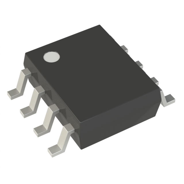
The BSO615N is a dual N-channel MOSFET array manufactured by Infineon Technologies, rated for 60V drain-source voltage with 2.6A continuous drain current. This component is classified as obsolete, necessitating identification of functionally equivalent alternatives for ongoing design support and production continuity. The part is housed in an 8-SOIC surface mount package and features logic level gate operation suitable for low-voltage switching applications.
Substiute Parts
Key Parameters
| Parameter | Value | Unit |
|---|---|---|
| Configuration | 2 N-Channel (Dual) | — |
| Drain to Source Voltage (Vdss) | 60 | V |
| Current - Continuous Drain (Id) @ 25°C | 2.6 | A |
| Rds On (Max) @ Id, Vgs | 150 mOhm @ 2.6A, 4.5V | — |
| Vgs(th) (Max) @ Id | 2 | V @ 20µA |
| Gate Charge (Qg) (Max) @ Vgs | 20 | nC @ 10V |
| Input Capacitance (Ciss) (Max) @ Vds | 380 | pF @ 25V |
| Power - Max | 2 | W |
| Operating Temperature Range | -55 to 150 | °C (TJ) |
| Mounting Type | Surface Mount | — |
| Package / Case | 8-SOIC (0.154", 3.90mm Width) | — |
| Product Status | Obsolete | — |
Substitute Part Grouping Explanation
Substitution of the BSO615N is determined by strict adherence to the following electrical and mechanical parameters:
Critical Matching Parameters:
- Dual N-channel MOSFET configuration
- 60V Vdss rating (minimum requirement)
- Continuous drain current capability ≥ 2.6A
- 8-SOIC surface mount package (0.154", 3.90mm width)
- Operating temperature range -55°C to 150°C
- Logic level gate operation
Acceptable Variation Parameters:
- Rds On values lower than 150 mOhm (improved performance)
- Gate charge lower than 20 nC (faster switching)
- Input capacitance variations within typical device tolerances
- Power dissipation capability ≥ 2W
All three substitute parts meet or exceed the critical matching parameters. Variations in secondary electrical characteristics represent performance improvements or equivalent specifications that do not compromise circuit functionality.
Parameter Comparison
| Parameter | BSO615N (Main) | PJL9830A_R2_00001 | STS4DNF60L | ZXMN6A11DN8TA |
|---|---|---|---|---|
| Manufacturer | Infineon Technologies | Panjit International Inc. | STMicroelectronics | Diodes Incorporated |
| Configuration | 2 N-Channel (Dual) | 2 N-Channel (Dual) | 2 N-Channel (Dual) | 2 N-Channel (Dual) |
| Vdss | 60V | 60V | 60V | 60V |
| Id @ 25°C | 2.6A | 4.8A (Ta) | 4A | 2.5A |
| Rds On (Max) | 150 mOhm @ 2.6A, 4.5V | 50 mOhm @ 4.8A, 10V | 55 mOhm @ 2A, 10V | 120 mOhm @ 2.5A, 10V |
| Vgs(th) (Max) | 2V @ 20µA | 2.5V @ 250µA | 2.5V @ 250µA | 1V @ 250µA (Min) |
| Gate Charge (Qg) (Max) | 20 nC @ 10V | 14 nC @ 10V | 15 nC @ 4.5V | 5.7 nC @ 10V |
| Ciss (Max) | 380 pF @ 25V | 815 pF @ 15V | 1030 pF @ 25V | 330 pF @ 40V |
| Power - Max | 2W | 2.5W (Ta) | 2W | 1.8W |
| Operating Temperature | -55 to 150°C (TJ) | -55 to 150°C (TJ) | -55 to 150°C (TJ) | -55 to 150°C (TJ) |
| Package / Case | 8-SOIC (0.154", 3.90mm Width) | 8-SOIC (0.154", 3.90mm Width) | 8-SOIC (0.154", 3.90mm Width) | 8-SOIC (0.154", 3.90mm Width) |
| Mounting Type | Surface Mount | Surface Mount | Surface Mount | Surface Mount |
| Product Status | Obsolete | Active | Active | Active |
| RoHS Status | Non-compliant | ROHS3 Compliant | ROHS3 Compliant | ROHS3 Compliant |
Engineering Selection Recommendations
STS4DNF60L (STMicroelectronics)
The STS4DNF60L is the primary substitute for the BSO615N. This part maintains identical package geometry (8-SOIC), matching Vdss (60V), and equivalent power rating (2W). The device features improved gate charge characteristics (15 nC versus 20 nC) and lower on-resistance (55 mOhm at 2A, 10V), resulting in reduced switching losses. The part is ROHS3 compliant with active product status and unlimited moisture sensitivity level (MSL 1), ensuring long-term availability and environmental compliance. The STripFET™ series designation indicates mature technology with established supply chain support.
PJL9830A_R2_00001 (Panjit International Inc.)
The PJL9830A_R2_00001 offers enhanced current handling capability (4.8A continuous drain current) with significantly reduced on-resistance (50 mOhm at 4.8A, 10V). This part is suitable for applications requiring higher current capacity within the same voltage class. The device is ROHS3 compliant and active in production. Higher input capacitance (815 pF at 15V) may impact switching speed in gate-drive-limited circuits. Packaging is supplied as Tape & Reel (TR).
ZXMN6A11DN8TA (Diodes Incorporated)
The ZXMN6A11DN8TA provides the lowest gate charge (5.7 nC at 10V) and lowest input capacitance (330 pF at 40V), making it optimal for high-frequency switching applications. Continuous drain current (2.5A) closely matches the BSO615N specification. On-resistance (120 mOhm at 2.5A, 10V) is slightly lower than the main part. The device is ROHS3 compliant with MSL 1 rating. Power dissipation capability (1.8W) is marginally lower than the main part but remains adequate for equivalent thermal management in most applications.
All three substitutes are ROHS3 compliant and REACH unaffected, addressing environmental and regulatory requirements that the obsolete BSO615N does not meet.
Frequently Asked Questions (FAQ)
Q: Can the STS4DNF60L directly replace the BSO615N in existing PCB layouts?
A: Yes. Both devices use identical 8-SOIC (0.154", 3.90mm width) packaging with matching pin configurations for dual N-channel MOSFET arrays. PCB footprints are interchangeable without modification.
Q: What is the primary advantage of the PJL9830A_R2_00001 over the BSO615N?
A: The PJL9830A_R2_00001 provides 4.8A continuous drain current versus 2.6A in the BSO615N, with significantly reduced on-resistance (50 mOhm versus 150 mOhm). This enables higher current switching applications and reduced power dissipation. The part is also ROHS3 compliant, addressing environmental compliance requirements.
Q: Which substitute is best for high-frequency switching circuits?
A: The ZXMN6A11DN8TA exhibits the lowest gate charge (5.7 nC) and input capacitance (330 pF), resulting in faster switching transitions and reduced gate drive power requirements. This part is optimal for applications operating above 100 kHz.
Q: Are all substitute parts available in the same packaging options as the BSO615N?
A: The STS4DNF60L and ZXMN6A11DN8TA are available in Cut Tape (CT) format. The PJL9830A_R2_00001 is supplied as Tape & Reel (TR). All three use 8-SOIC surface mount packages with identical footprints.
Q: What is the moisture sensitivity level (MSL) difference between the main part and substitutes?
A: The BSO615N has MSL 3 (168 hours), indicating higher moisture absorption risk. All three substitutes have MSL 1 (unlimited), providing superior moisture resistance and extended shelf life without baking requirements.
Q: Can the ZXMN6A11DN8TA be used in applications requiring the full 2.6A continuous current of the BSO615N?
A: The ZXMN6A11DN8TA is rated for 2.5A continuous drain current, which is within 96% of the BSO615N specification. For applications requiring exactly 2.6A or higher, the PJL9830A_R2_00001 (4.8A) or STS4DNF60L (4A) are more appropriate selections.
Q: What is the impact of higher input capacitance in the PJL9830A_R2_00001?
A: The PJL9830A_R2_00001 has input capacitance of 815 pF at 15V, compared to 380 pF in the BSO615N. Higher capacitance increases gate charge time and requires higher gate drive current. This affects switching speed and power consumption in gate-drive-limited circuits but does not impact DC switching capability.
Q: Are all substitutes suitable for the full -55°C to 150°C operating temperature range?
A: Yes. All three substitute parts are rated for -55°C to 150°C junction temperature (TJ), matching the BSO615N specification and ensuring thermal compatibility across the full operating range.
Alternative Parts

SJ6012L2TP
Littelfuse Inc.
6 Alternative Parts

JMK107BBJ476MA-RE
Taiyo Yuden
10 Alternative Parts

GMK107BBJ475MA-T
Taiyo Yuden
5 Alternative Parts
SJ6020N2ARP
Littelfuse Inc.
3 Alternative Parts
SJ6025R2ATP
Littelfuse Inc.
4 Alternative Parts

2474-05L
API Delevan Inc.
1 Alternative Parts

4590R-684K
API Delevan Inc.
1 Alternative Parts

CM6560R-334
API Delevan Inc.
1 Alternative Parts

CM6460-104
API Delevan Inc.
1 Alternative Parts

5526-12
API Delevan Inc.
1 Alternative Parts