


Request Quote
(Ships tomorrow)
ATP613-TL-H Equivalent & Substitute Parts
Part Overview
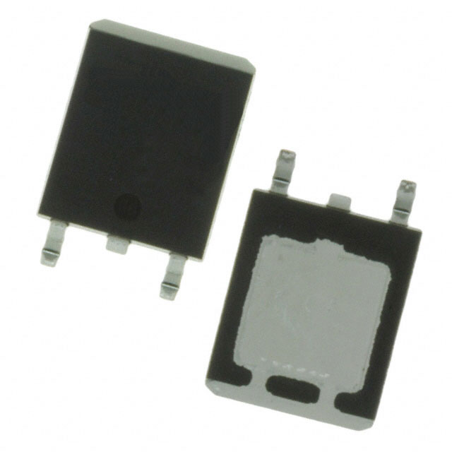
The ATP613-TL-H is an N-Channel 500V 5.5A MOSFET manufactured by onsemi in ATPAK surface mount packaging. This device is classified as obsolete, necessitating identification of equivalent alternatives for ongoing design requirements and production continuity. The part delivers 70W maximum power dissipation at case temperature and operates at junction temperatures up to 150°C. Equivalent substitutes must maintain compatibility with the 500V drain-source voltage rating and support comparable continuous drain current specifications while accommodating different package formats.
Substiute Parts
Key Parameters
| Parameter | ATP613-TL-H | Unit |
|---|---|---|
| Manufacturer | onsemi | — |
| FET Type | N-Channel | — |
| Technology | MOSFET (Metal Oxide) | — |
| Drain to Source Voltage (Vdss) | 500 | V |
| Continuous Drain Current (Id) @ 25°C | 5.5 | A (Ta) |
| Rds On (Max) @ Id, Vgs | 2 | Ω @ 2.75A, 10V |
| Gate Charge (Qg) @ Vgs | 13.8 | nC @ 10V |
| Vgs (Max) | ±30 | V |
| Input Capacitance (Ciss) @ Vds | 350 | pF @ 30V |
| Power Dissipation (Max) | 70 | W (Tc) |
| Operating Temperature (TJ) | 150 | °C |
| Mounting Type | Surface Mount | — |
| Package / Case | ATPAK (2 Leads+Tab) | — |
| Product Status | Obsolete | — |
| Moisture Sensitivity Level (MSL) | 1 (Unlimited) | — |
Substitute Part Grouping Explanation
Substitution of the ATP613-TL-H is determined by the following critical electrical and mechanical parameters:
Primary Substitution Criteria:
- Drain to Source Voltage (Vdss): 500V minimum (higher ratings acceptable)
- Continuous Drain Current (Id): Minimum 4A at rated conditions (5.5A preferred for direct replacement)
- On-State Resistance (Rds On): Maximum 2.5Ω at specified gate voltage
- Gate Charge (Qg): Maximum 25 nC at 10V gate voltage
- Maximum Gate Voltage (Vgs): ±20V minimum (±30V preferred)
- Power Dissipation: Minimum 70W at case temperature
- Operating Temperature: 150°C junction temperature minimum
- Mounting Type: Surface Mount required
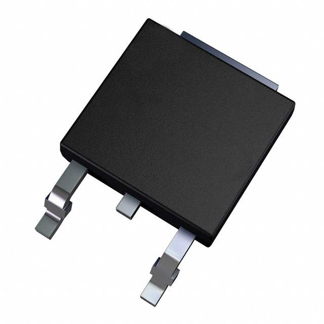
- Package Format: ATPAK, DPAK, or TO-252 acceptable
The substitute parts listed below satisfy these criteria within the specified electrical and thermal operating ranges. Package format differences are accommodated through standard PCB layout modifications without affecting electrical performance.
Parameter Comparison
| Parameter | ATP613-TL-H (onsemi) | IXTY1R6N50D2 (IXYS) | TK4P50D(T6RSS-Q) (Toshiba) | TK4P55DA(T6RSS-Q) (Toshiba) | Unit |
|---|---|---|---|---|---|
| Drain to Source Voltage (Vdss) | 500 | 500 | 500 | 550 | V |
| Continuous Drain Current (Id) @ 25°C | 5.5 (Ta) | 1.6 (Tc) | 4 (Ta) | 3.5 (Ta) | A |
| Rds On (Max) @ Id, Vgs | 2 @ 2.75A, 10V | 2.3 @ 800mA, 0V | 2 @ 2A, 10V | 2.45 @ 1.8A, 10V | Ω |
| Gate Charge (Qg) @ Vgs | 13.8 @ 10V | 23.7 @ 5V | 9 @ 10V | 9 @ 10V | nC |
| Vgs (Max) | ±30 | ±20 | ±30 | ±30 | V |
| Input Capacitance (Ciss) @ Vds | 350 @ 30V | 645 @ 25V | 380 @ 25V | 380 @ 25V | pF |
| Power Dissipation (Max) | 70 (Tc) | 100 (Tc) | 80 (Tc) | 80 (Tc) | W |
| Operating Temperature (TJ) | 150 | 150 | 150 | 150 | °C |
| Mounting Type | Surface Mount | Surface Mount | Surface Mount | Surface Mount | — |
| Package / Case | ATPAK (2 Leads+Tab) | TO-252-3, DPAK (2 Leads + Tab), SC-63 | TO-252-3, DPAK (2 Leads + Tab), SC-63 | TO-252-3, DPAK (2 Leads + Tab), SC-63 | — |
| Product Status | Obsolete | Active | Active | Active | — |
Engineering Selection Recommendations
IXTY1R6N50D2 (IXYS): This part maintains the 500V Vdss rating and surface mount configuration. However, the continuous drain current rating of 1.6A (Tc) is significantly lower than the ATP613-TL-H specification of 5.5A (Ta). This device is suitable only for applications where current requirements do not exceed 1.6A. The part is active and available in high inventory (6698 pcs). Package format is TO-252AA, requiring PCB layout modification. Gate charge is elevated at 23.7 nC compared to the original 13.8 nC specification.
TK4P50D(T6RSS-Q) (Toshiba Semiconductor and Storage): This part provides the closest electrical match to the ATP613-TL-H. It maintains 500V Vdss, delivers 4A continuous drain current (Ta), and achieves 2Ω on-state resistance at 2A and 10V gate voltage. Gate charge is reduced to 9 nC at 10V, improving switching performance. The device is RoHS Compliant and active in production. Package format is DPAK (TO-252-3), compatible with standard surface mount assembly. Inventory availability is 843 pcs. This part is recommended for direct substitution in applications where 4A current capacity is sufficient.
TK4P55DA(T6RSS-Q) (Toshiba Semiconductor and Storage): This part offers a higher voltage rating of 550V Vdss, providing additional design margin. Continuous drain current is 3.5A (Ta), lower than the original 5.5A specification. On-state resistance is 2.45Ω at 1.8A and 10V gate voltage. Gate charge remains at 9 nC at 10V. The device is RoHS Compliant and active in production with high inventory availability (3400 pcs). Package format is DPAK (TO-252-3). This part is suitable for applications requiring higher voltage headroom with reduced current requirements.
All substitute parts maintain MSL 1 (Unlimited) moisture sensitivity classification and surface mount assembly compatibility. Selection between TK4P50D and TK4P55DA depends on application current and voltage requirements.
Frequently Asked Questions (FAQ)
Q: Can the IXTY1R6N50D2 directly replace the ATP613-TL-H?
A: The IXTY1R6N50D2 maintains the 500V voltage rating and surface mount configuration. However, the continuous drain current specification of 1.6A is substantially lower than the ATP613-TL-H rating of 5.5A. Direct replacement is limited to applications where maximum current does not exceed 1.6A. The elevated gate charge of 23.7 nC also affects switching characteristics compared to the original 13.8 nC specification.
Q: What is the primary difference between the two Toshiba substitute options?
A: The TK4P50D(T6RSS-Q) maintains the 500V voltage rating with 4A continuous drain current. The TK4P55DA(T6RSS-Q) provides a higher 550V voltage rating with 3.5A continuous drain current. Both devices share identical gate charge (9 nC) and on-state resistance characteristics at their respective rated currents. Selection depends on whether the application requires the higher voltage margin or the additional current capacity.
Q: Are package format differences between ATPAK and DPAK significant for substitution?
A: Package format differences require PCB layout modifications but do not affect electrical performance. Both ATPAK and DPAK (TO-252-3) are surface mount packages with identical lead configurations (2 Leads + Tab). Standard PCB footprint conversion tools accommodate the transition. Thermal performance remains equivalent when proper PCB copper area and thermal vias are implemented according to package specifications.
Q: Which substitute part is recommended for new designs?
A: The TK4P50D(T6RSS-Q) provides the closest electrical match to the ATP613-TL-H with 4A continuous drain current, 2Ω on-state resistance, and reduced gate charge of 9 nC. This part is active in production, RoHS Compliant, and available in high inventory. It is suitable for applications where 4A current capacity meets design requirements. The TK4P55DA(T6RSS-Q) is recommended when higher voltage margin (550V) is required and current requirements are 3.5A or lower.
Q: What compliance certifications apply to the substitute parts?
A: The TK4P50D(T6RSS-Q) and TK4P55DA(T6RSS-Q) are both RoHS Compliant. All parts listed maintain REACH Unaffected status and EAR99 ECCN classification. MSL 1 (Unlimited) moisture sensitivity applies to all devices, eliminating special handling requirements during assembly and storage.
Q: How do gate charge differences affect circuit design?
A: Gate charge (Qg) determines the energy required to switch the MOSFET on and off. The ATP613-TL-H specifies 13.8 nC at 10V. The TK4P50D and TK4P55DA both specify 9 nC at 10V, reducing switching losses and improving efficiency. The IXTY1R6N50D2 specifies 23.7 nC at 5V, increasing switching energy requirements. Gate driver circuits must supply sufficient current to charge the gate within the required switching time window.
Q: Can the ATP613-TL-H be used in applications requiring higher than 500V operation?
A: No. The ATP613-TL-H is rated for maximum 500V drain-source voltage. The TK4P55DA(T6RSS-Q) provides a 550V rating for applications requiring higher voltage operation. Exceeding the rated Vdss specification results in device failure and potential circuit damage.
Alternative Parts

SJ6012L2TP
Littelfuse Inc.
6 Alternative Parts

JMK107BBJ476MA-RE
Taiyo Yuden
10 Alternative Parts

GMK107BBJ475MA-T
Taiyo Yuden
5 Alternative Parts
SJ6020N2ARP
Littelfuse Inc.
3 Alternative Parts
SJ6025R2ATP
Littelfuse Inc.
4 Alternative Parts

2474-05L
API Delevan Inc.
1 Alternative Parts

4590R-684K
API Delevan Inc.
1 Alternative Parts

CM6560R-334
API Delevan Inc.
1 Alternative Parts

CM6460-104
API Delevan Inc.
1 Alternative Parts

5526-12
API Delevan Inc.
1 Alternative Parts