


Request Quote
(Ships tomorrow)
ATP202-TL-H Equivalent & Substitute Parts
Part Overview
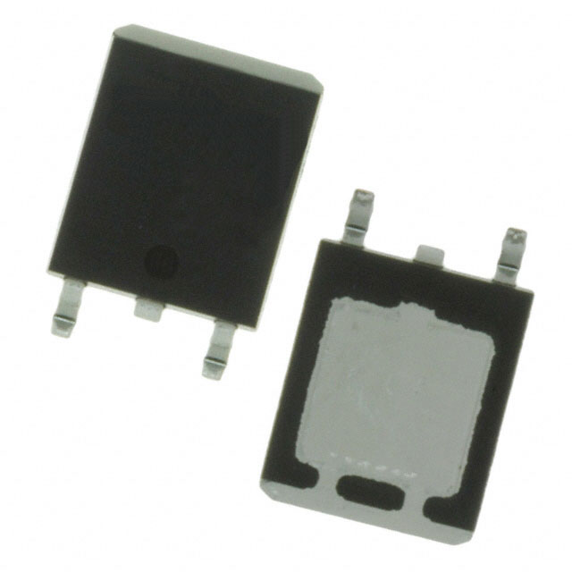
The ATP202-TL-H is an N-Channel MOSFET manufactured by onsemi, rated for 30V drain-to-source voltage with 50A continuous drain current at 25°C (Ta) in the ATPAK surface mount package. This device is classified as obsolete, necessitating identification of functionally equivalent alternatives for ongoing design support and procurement continuity. The ATPAK package configuration and specific electrical characteristics require careful evaluation when selecting substitute components.
Substiute Parts
Key Parameters
| Parameter | Value | Unit |
|---|---|---|
| Drain-to-Source Voltage (Vdss) | 30 | V |
| Continuous Drain Current @ 25°C (Ta) | 50 | A |
| On-State Resistance (Rds On) @ 25A, 10V | 12 | mOhm |
| Gate Charge (Qg) @ 10V | 27 | nC |
| Input Capacitance (Ciss) @ 10V | 1650 | pF |
| Maximum Gate Voltage (Vgs) | ±20 | V |
| Power Dissipation (Tc) | 40 | W |
| Operating Temperature (TJ) | 150 | °C |
| Package Type | ATPAK (2 Leads+Tab) | — |
| Mounting Type | Surface Mount | — |
| RoHS Status | ROHS3 Compliant | — |
| Moisture Sensitivity Level | 1 (Unlimited) | — |
Substitute Part Grouping Explanation
Substitution of the ATP202-TL-H is determined by equivalence across the following critical parameters:
Electrical Equivalence Criteria:
- Drain-to-Source Voltage (Vdss): Must equal or exceed 30V
- Continuous Drain Current (Id @ 25°C): Must meet or exceed 50A at Ta rating
- On-State Resistance (Rds On): Must not exceed 12mOhm at specified gate voltage
- Gate Charge (Qg): Lower values indicate faster switching characteristics
- Input Capacitance (Ciss): Affects gate drive requirements
- Maximum Gate Voltage (Vgs): Must accommodate ±20V operation
Mechanical and Compliance Criteria:
- Package Type: ATPAK configuration with 2 leads and tab
- Surface Mount compatibility
- RoHS3 compliance
- Moisture Sensitivity Level 1 (Unlimited)
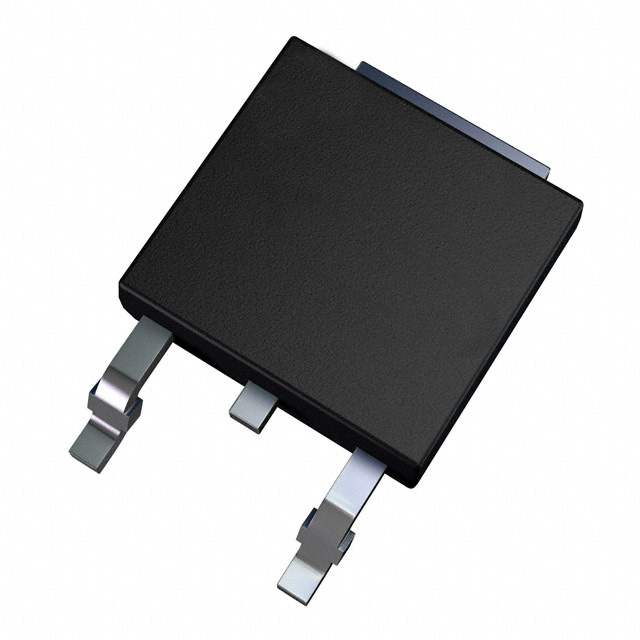
The FDD6690A is identified as a manufacturer-recommended substitute. While it operates at the same 30V Vdss rating and maintains equivalent Rds On characteristics, it utilizes a different package format (TO-252AA/DPAK) and exhibits different current ratings under Ta and Tc conditions. This substitution requires mechanical redesign of the printed circuit board layout to accommodate the alternative package geometry.
Parameter Comparison
| Parameter | ATP202-TL-H | FDD6690A | Unit |
|---|---|---|---|
| Manufacturer | onsemi | onsemi | — |
| FET Type | N-Channel | N-Channel | — |
| Technology | MOSFET (Metal Oxide) | MOSFET (Metal Oxide) | — |
| Drain-to-Source Voltage (Vdss) | 30 | 30 | V |
| Continuous Drain Current @ 25°C (Ta) | 50 | 12 | A |
| Continuous Drain Current (Tc) | — | 46 | A |
| On-State Resistance (Rds On) @ 10V | 12 @ 25A | 12 @ 12A | mOhm |
| Gate Charge (Qg) | 27 @ 10V | 18 @ 5V | nC |
| Input Capacitance (Ciss) | 1650 @ 10V | 1230 @ 15V | pF |
| Maximum Gate Voltage (Vgs) | ±20 | ±20 | V |
| Power Dissipation (Tc) | 40 | 56 | W |
| Operating Temperature Range (TJ) | —55 to 150 | —55 to 175 | °C |
| Package Type | ATPAK (2 Leads+Tab) | TO-252-3, DPAK (2 Leads+Tab) | — |
| Mounting Type | Surface Mount | Surface Mount | — |
| RoHS Status | ROHS3 Compliant | ROHS3 Compliant | — |
| Moisture Sensitivity Level | 1 (Unlimited) | 1 (Unlimited) | — |
| Product Status | Obsolete | Obsolete | — |
Engineering Selection Recommendations
Compliance and Regulatory Status: Both the ATP202-TL-H and FDD6690A are ROHS3 compliant and REACH unaffected, meeting current environmental and regulatory requirements for electronic component procurement. Both devices carry Moisture Sensitivity Level 1 (Unlimited), indicating no special moisture handling requirements during storage or assembly.
Product Status Consideration: Both components are classified as obsolete. Selection between these parts should account for long-term availability and supply chain planning. The FDD6690A maintains higher inventory levels (38,065 pieces) compared to the ATP202-TL-H (1,715 pieces), which may influence procurement strategy for high-volume applications.
Electrical Performance: The ATP202-TL-H delivers 50A continuous drain current at Ta, while the FDD6690A is rated for 12A at Ta but 46A at Tc. The on-state resistance specification of 12mOhm is identical for both devices at their respective rated currents and gate voltages. Gate charge and input capacitance values differ, affecting gate drive circuit design and switching speed characteristics.
Package Compatibility: The ATP202-TL-H uses the ATPAK package, while the FDD6690A uses the TO-252-3 (DPAK) package. These are mechanically incompatible, requiring circuit board redesign if substitution is implemented. Pin configuration and thermal tab placement differ between packages.
Temperature Operating Range: The FDD6690A extends the maximum junction temperature to 175°C compared to the ATP202-TL-H at 150°C, providing additional thermal margin in high-temperature applications.
Frequently Asked Questions (FAQ)
Q: Can the FDD6690A directly replace the ATP202-TL-H without circuit board modification?
A: No. The ATP202-TL-H uses the ATPAK package while the FDD6690A uses the TO-252-3 (DPAK) package. These packages have different footprints, pin spacing, and thermal tab configurations. Circuit board layout redesign is required for mechanical compatibility.
Q: Are the electrical characteristics of both devices equivalent?
A: Both devices share identical drain-to-source voltage (30V) and on-state resistance (12mOhm) specifications. However, they differ in continuous drain current ratings under Ta conditions (50A vs. 12A) and gate charge values (27nC vs. 18nC). Application-specific current requirements determine suitability.
Q: What is the significance of the Ta versus Tc current rating difference?
A: Ta (ambient temperature) and Tc (case temperature) represent different measurement conditions. The ATP202-TL-H specifies 50A at Ta, while the FDD6690A specifies 12A at Ta and 46A at Tc. For applications requiring sustained 50A operation at ambient temperature, the ATP202-TL-H rating is more directly applicable.
Q: Do both devices require identical gate drive circuits?
A: Both devices accept ±20V maximum gate voltage and operate with similar gate voltage thresholds. However, gate charge differences (27nC vs. 18nC) affect gate drive current requirements and switching speed. Gate drive circuit redesign may be necessary to optimize performance with the substitute device.
Q: Are there moisture handling differences between these components?
A: No. Both devices carry Moisture Sensitivity Level 1 (Unlimited), indicating identical moisture handling requirements. Standard surface mount assembly processes apply to both components without additional precautions.
Q: What is the impact of the different operating temperature ranges?
A: The FDD6690A supports operation to 175°C junction temperature, compared to 150°C for the ATP202-TL-H. This provides 25°C additional thermal margin. For applications operating near thermal limits, the FDD6690A offers improved temperature headroom.
Q: Are both devices suitable for new design implementations?
A: Both components are classified as obsolete. For new designs, evaluation of currently active alternatives from the onsemi product portfolio is recommended to ensure long-term supply availability and support.
Alternative Parts

SJ6012L2TP
Littelfuse Inc.
6 Alternative Parts

JMK107BBJ476MA-RE
Taiyo Yuden
10 Alternative Parts

GMK107BBJ475MA-T
Taiyo Yuden
5 Alternative Parts
SJ6020N2ARP
Littelfuse Inc.
3 Alternative Parts
SJ6025R2ATP
Littelfuse Inc.
4 Alternative Parts

2474-05L
API Delevan Inc.
1 Alternative Parts

4590R-684K
API Delevan Inc.
1 Alternative Parts

CM6560R-334
API Delevan Inc.
1 Alternative Parts

CM6460-104
API Delevan Inc.
1 Alternative Parts

5526-12
API Delevan Inc.
1 Alternative Parts