


Request Quote
(Ships tomorrow)
ATP201-TL-H N-Channel MOSFET Equivalent & Substitute Parts
Part Overview
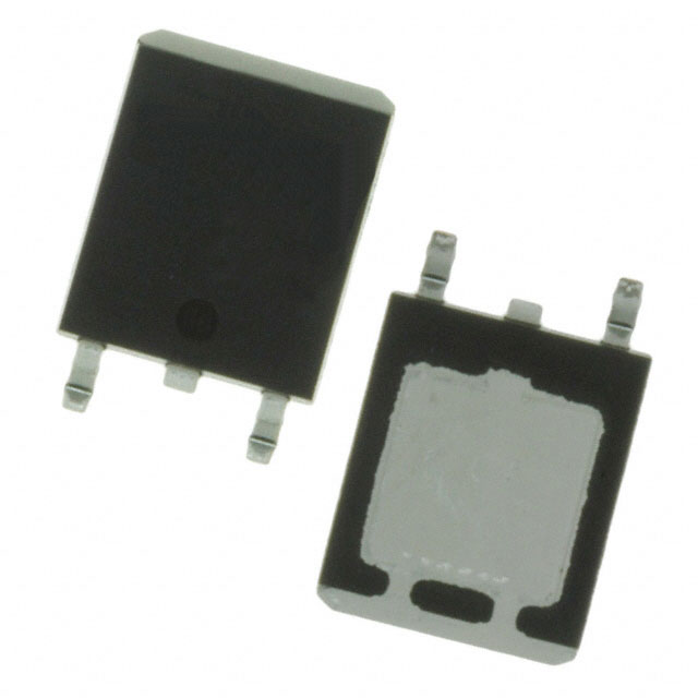
The ATP201-TL-H is an N-Channel 30V 35A surface mount MOSFET manufactured by onsemi in the ATPAK package. This device is classified as obsolete product status. Identifying equivalent and substitute parts is necessary to maintain design continuity, ensure supply chain availability, and support ongoing production requirements for applications utilizing this component.
Substiute Parts
Key Parameters
| Parameter | Value | Unit |
|---|---|---|
| Manufacturer Part Number | ATP201-TL-H | — |
| Manufacturer | onsemi | — |
| FET Type | N-Channel | — |
| Technology | MOSFET (Metal Oxide) | — |
| Drain to Source Voltage (Vdss) | 30 | V |
| Continuous Drain Current (Id) @ 25°C | 35 | A (Ta) |
| Rds On (Max) @ Id, Vgs | 17 | mOhm @ 18A, 10V |
| Gate Charge (Qg) (Max) @ Vgs | 17 | nC @ 10V |
| Vgs (Max) | ±20 | V |
| Input Capacitance (Ciss) (Max) @ Vds | 985 | pF @ 10V |
| Power Dissipation (Max) | 30 | W (Tc) |
| Operating Temperature (TJ) | 150 | °C |
| Mounting Type | Surface Mount | — |
| Package / Case | ATPAK (2 Leads+Tab) | — |
| Moisture Sensitivity Level (MSL) | 1 (Unlimited) | — |
| Product Status | Obsolete | — |
Substitute Part Grouping Explanation
Substitution of the ATP201-TL-H is determined by strict alignment of the following electrical and mechanical parameters:
Critical Matching Parameters:
- FET Type: N-Channel
- Technology: MOSFET (Metal Oxide)
- Drain to Source Voltage (Vdss): 30V
- Mounting Type: Surface Mount
- Package / Case: ATPAK (2 Leads+Tab)
- Gate Drive Voltage: 10V nominal
Allowable Variation Parameters:
- Continuous Drain Current (Id): Equal to or greater than 35A
- Rds On (Max): Equal to or lower than 17 mOhm
- Gate Charge (Qg): Equal to or lower than 17 nC
- Input Capacitance (Ciss): Equal to or lower than 985 pF
- Power Dissipation (Max): Equal to or greater than 30W
The ATP202-TL-H qualifies as a direct substitute based on these criteria. It maintains identical voltage ratings, package configuration, and gate drive specifications while providing enhanced current handling (50A vs. 35A), improved on-resistance (12 mOhm vs. 17 mOhm), and increased power dissipation capability (40W vs. 30W).
Parameter Comparison
| Parameter | ATP201-TL-H | ATP202-TL-H | Unit |
|---|---|---|---|
| Manufacturer | onsemi | onsemi | — |
| FET Type | N-Channel | N-Channel | — |
| Technology | MOSFET (Metal Oxide) | MOSFET (Metal Oxide) | — |
| Drain to Source Voltage (Vdss) | 30 | 30 | V |
| Continuous Drain Current (Id) @ 25°C | 35 | 50 | A (Ta) |
| Rds On (Max) @ Id, Vgs | 17 @ 18A, 10V | 12 @ 25A, 10V | mOhm |
| Gate Charge (Qg) (Max) @ Vgs | 17 | 27 | nC @ 10V |
| Vgs (Max) | ±20 | ±20 | V |
| Input Capacitance (Ciss) (Max) @ Vds | 985 | 1650 | pF @ 10V |
| Power Dissipation (Max) | 30 | 40 | W (Tc) |
| Operating Temperature (TJ) | 150 | 150 | °C |
| Mounting Type | Surface Mount | Surface Mount | — |
| Package / Case | ATPAK (2 Leads+Tab) | ATPAK (2 Leads+Tab) | — |
| Moisture Sensitivity Level (MSL) | 1 (Unlimited) | 1 (Unlimited) | — |
| Product Status | Obsolete | Obsolete | — |
Engineering Selection Recommendations
ATP202-TL-H as Primary Substitute:
The ATP202-TL-H is a direct functional substitute for the ATP201-TL-H. Both devices share identical voltage ratings (30V Vdss), gate drive specifications (±20V Vgs Max), package configuration (ATPAK), and thermal operating range (150°C TJ). Both are classified as obsolete products with MSL 1 (Unlimited) moisture sensitivity rating.
The ATP202-TL-H provides performance enhancements across all critical parameters: increased continuous drain current (50A vs. 35A), reduced on-resistance (12 mOhm vs. 17 mOhm), and higher power dissipation capability (40W vs. 30W). These improvements ensure the substitute part meets or exceeds the electrical requirements of the original design.
Both devices are REACH Unaffected and classified under ECCN EAR99, maintaining equivalent regulatory compliance status.
Compliance Considerations:
The ATP202-TL-H carries RoHS3 Compliant certification, whereas the ATP201-TL-H compliance status is not specified in available documentation. This represents an improvement in environmental compliance for designs requiring RoHS certification.
Frequently Asked Questions (FAQ)
Q: Can the ATP202-TL-H directly replace the ATP201-TL-H in existing designs?
A: Yes. The ATP202-TL-H is a direct substitute. Both devices maintain identical Vdss (30V), Vgs (±20V), package configuration (ATPAK), and thermal specifications (150°C TJ). The ATP202-TL-H provides equal or superior electrical performance across all parameters.
Q: What are the key differences between ATP201-TL-H and ATP202-TL-H?
A: The ATP202-TL-H provides higher continuous drain current (50A vs. 35A), lower on-resistance (12 mOhm vs. 17 mOhm), and greater power dissipation capability (40W vs. 30W). Gate charge is higher (27 nC vs. 17 nC) and input capacitance is higher (1650 pF vs. 985 pF). These differences reflect an enhanced device within the same product family.
Q: Are there any package or pinout differences between these parts?
A: No. Both ATP201-TL-H and ATP202-TL-H use identical ATPAK (2 Leads+Tab) surface mount packaging. Pinout and mechanical dimensions are identical, enabling direct PCB-level substitution without layout modifications.
Q: What is the significance of the obsolete product status?
A: Both the ATP201-TL-H and ATP202-TL-H are classified as obsolete. This status indicates these devices are no longer in active production. Substitution between these parts addresses supply continuity within the obsolete product family. For new designs, evaluation of current-generation alternatives is recommended.
Q: Do both parts have the same moisture sensitivity rating?
A: Yes. Both ATP201-TL-H and ATP202-TL-H carry MSL 1 (Unlimited) rating, indicating no moisture sensitivity restrictions for storage, handling, or reflow processes.
Q: Are there regulatory or compliance differences between the two parts?
A: Both parts are REACH Unaffected and classified under ECCN EAR99. The ATP202-TL-H carries RoHS3 Compliant certification. For applications requiring RoHS compliance, the ATP202-TL-H provides documented compliance status.
Q: What gate drive voltage should be used with these MOSFETs?
A: Both devices specify 10V as the nominal gate drive voltage for minimum on-resistance specification. Maximum gate voltage is ±20V for both parts. Gate drive circuits must not exceed these voltage limits.
Alternative Parts

SJ6012L2TP
Littelfuse Inc.
6 Alternative Parts

JMK107BBJ476MA-RE
Taiyo Yuden
10 Alternative Parts

GMK107BBJ475MA-T
Taiyo Yuden
5 Alternative Parts
SJ6020N2ARP
Littelfuse Inc.
3 Alternative Parts
SJ6025R2ATP
Littelfuse Inc.
4 Alternative Parts

2474-05L
API Delevan Inc.
1 Alternative Parts

4590R-684K
API Delevan Inc.
1 Alternative Parts

CM6560R-334
API Delevan Inc.
1 Alternative Parts

CM6460-104
API Delevan Inc.
1 Alternative Parts

5526-12
API Delevan Inc.
1 Alternative Parts