


Request Quote
(Ships tomorrow)
ATP113-TL-H Equivalent & Substitute Parts
Part Overview
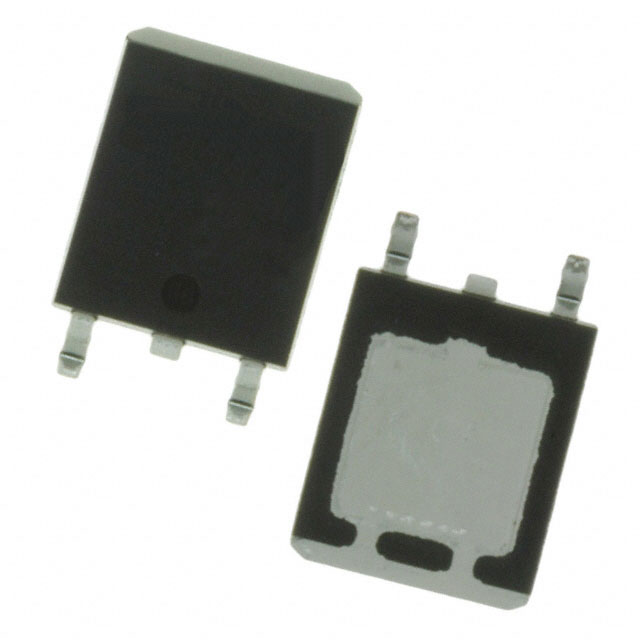
The ATP113-TL-H is an active P-Channel MOSFET manufactured by onsemi, rated for 60V drain-to-source voltage with 35A continuous drain current at 25°C. The device is housed in an ATPAK surface mount package and is designed for applications requiring moderate power dissipation up to 50W (Tc). This component is ROHS3 compliant and carries an unlimited moisture sensitivity level (MSL 1).
Substitute parts are identified when equivalent electrical performance and mechanical compatibility can be maintained across the specified parameter ranges. Alternative models may be required due to inventory constraints, supply chain considerations, or design optimization for specific thermal or packaging requirements.
Substiute Parts
Key Parameters
| Parameter | ATP113-TL-H | Unit |
|---|---|---|
| Drain-to-Source Voltage (Vdss) | 60 | V |
| Continuous Drain Current (Id) @ 25°C | 35 | A |
| Rds On (Max) @ 18A, 10V | 29.5 | mOhm |
| Gate Charge (Qg) @ 10V | 55 | nC |
| Input Capacitance (Ciss) @ 20V | 2400 | pF |
| Power Dissipation (Max) @ Tc | 50 | W |
| Operating Temperature (TJ) | 150 | °C |
| Package Type | ATPAK (2 Leads+Tab) | — |
| FET Type | P-Channel | — |
| Technology | MOSFET (Metal Oxide) | — |
Substitute Part Grouping Explanation
Substitute parts for the ATP113-TL-H are qualified based on the following electrical and mechanical criteria:
Primary Substitution Criteria:
- Drain-to-Source Voltage (Vdss): 60V minimum
- Continuous Drain Current (Id): 35A or greater at rated temperature
- Gate-Source Voltage (Vgs): ±20V maximum rating
- FET Type: P-Channel configuration
- Technology: MOSFET (Metal Oxide)
- Mounting Type: Surface Mount
- Compliance: ROHS3 compliant, MSL 1 (Unlimited)
Secondary Compatibility Parameters:
- Rds On (Max): Within acceptable range for switching and conduction losses
- Gate Charge (Qg): Influences switching speed and drive requirements
- Input Capacitance (Ciss): Affects gate drive circuit design
- Power Dissipation: Thermal capability for application requirements
- Operating Temperature: Maximum junction temperature rating
The substitute parts listed maintain electrical equivalence within the specified parameter envelope while accommodating variations in package form factor and thermal performance characteristics.
Parameter Comparison
| Parameter | ATP113-TL-H (onsemi) | STD35P6LLF6 (STMicroelectronics) | NP36P06SLG-E1-AY (Renesas) | Unit |
|---|---|---|---|---|
| Drain-to-Source Voltage (Vdss) | 60 | 60 | 60 | V |
| Continuous Drain Current (Id) @ 25°C | 35 (Ta) | 35 (Tc) | 36 (Tc) | A |
| Rds On (Max) @ 10V | 29.5 @ 18A | 28 @ 17.5A | 30 @ 18A | mOhm |
| Gate Charge (Qg) @ Vgs | 55 @ 10V | 30 @ 4.5V | 52 @ 10V | nC |
| Input Capacitance (Ciss) | 2400 @ 20V | 3780 @ 25V | 3200 @ 10V | pF |
| Power Dissipation (Max) @ Tc | 50 | 70 | 56 | W |
| Operating Temperature (TJ) | 150 | 175 | 175 | °C |
| Package Type | ATPAK (2 Leads+Tab) | DPAK (2 Leads+Tab) | TO-252 (2 Leads+Tab) | — |
| FET Type | P-Channel | P-Channel | P-Channel | — |
| Technology | MOSFET (Metal Oxide) | MOSFET (Metal Oxide) | MOSFET (Metal Oxide) | — |
| Vgs (Max) | ±20 | ±20 | ±20 | V |
| RoHS Status | ROHS3 Compliant | ROHS3 Compliant | ROHS3 Compliant | — |
| MSL Rating | 1 (Unlimited) | 1 (Unlimited) | 1 (Unlimited) | — |
Engineering Selection Recommendations
STD35P6LLF6 (STMicroelectronics)
The STD35P6LLF6 is a direct electrical equivalent with identical 60V/35A ratings and superior thermal performance (70W vs. 50W). The device features lower gate charge (30 nC @ 4.5V) compared to the ATP113-TL-H, resulting in faster switching characteristics. Operating temperature extends to 175°C, providing additional thermal margin. The DPAK package offers equivalent thermal and electrical performance to ATPAK. This part is ROHS3 compliant with MSL 1 rating. Inventory availability is substantial (32,820 pcs).
NP36P06SLG-E1-AY (Renesas Electronics Corporation)
The NP36P06SLG-E1-AY provides a 60V/36A rating with marginally higher current capability. Rds On performance is comparable (30 mOhm @ 18A, 10V). Power dissipation reaches 56W (Tc), exceeding the ATP113-TL-H specification. Operating temperature is rated to 175°C. The TO-252 package is mechanically compatible with DPAK and ATPAK form factors. This device is ROHS3 compliant with MSL 1 rating. Inventory availability is adequate (1,718 pcs).
All substitute parts maintain active product status, full regulatory compliance (ROHS3, REACH unaffected, EAR99 classification), and unlimited moisture sensitivity rating.
Frequently Asked Questions (FAQ)
Q: Can the STD35P6LLF6 replace the ATP113-TL-H in existing designs?
A: Yes. Both devices share identical electrical specifications (60V/35A) and are P-Channel MOSFETs with ±20V gate-source voltage ratings. The STD35P6LLF6 offers superior thermal performance (70W vs. 50W) and lower gate charge. Package form factors (DPAK vs. ATPAK) are mechanically compatible in surface mount applications. PCB layout and thermal management considerations remain equivalent.
Q: What are the key differences between the NP36P06SLG-E1-AY and ATP113-TL-H?
A: The NP36P06SLG-E1-AY provides 36A continuous drain current versus 35A, with comparable Rds On performance (30 mOhm vs. 29.5 mOhm). Power dissipation is higher (56W vs. 50W). The TO-252 package is mechanically similar to ATPAK. Gate charge is slightly lower (52 nC vs. 55 nC). Both devices operate at ±20V maximum gate-source voltage and are ROHS3 compliant.
Q: Are package differences between ATPAK, DPAK, and TO-252 significant for substitution?
A: ATPAK, DPAK, and TO-252 are all surface mount packages with two leads plus a tab configuration. Thermal and electrical performance are equivalent across these package types. PCB footprint dimensions differ; verify land pattern compatibility with your design before substitution. All three packages provide equivalent heat dissipation characteristics for the specified power ratings.
Q: Do all substitute parts meet the same compliance requirements?
A: Yes. The ATP113-TL-H, STD35P6LLF6, and NP36P06SLG-E1-AY are all ROHS3 compliant, REACH unaffected, and carry EAR99 classification. All devices have MSL 1 (Unlimited) moisture sensitivity ratings. Regulatory and environmental compliance is equivalent across all three parts.
Q: Which substitute offers the best thermal performance?
A: The STD35P6LLF6 provides the highest power dissipation rating at 70W (Tc), compared to 50W for the ATP113-TL-H and 56W for the NP36P06SLG-E1-AY. The STD35P6LLF6 also features the highest operating temperature rating at 175°C (TJ). For applications requiring maximum thermal headroom, the STD35P6LLF6 is the optimal selection.
Q: How do gate charge differences affect circuit design?
A: The STD35P6LLF6 has significantly lower gate charge (30 nC @ 4.5V) compared to the ATP113-TL-H (55 nC @ 10V) and NP36P06SLG-E1-AY (52 nC @ 10V). Lower gate charge reduces switching losses and allows faster switching transitions. Gate drive circuit design may require adjustment to accommodate these differences, particularly in high-frequency applications. Verify gate drive voltage and current capabilities with your specific circuit topology.
Alternative Parts

SJ6012L2TP
Littelfuse Inc.
6 Alternative Parts

JMK107BBJ476MA-RE
Taiyo Yuden
10 Alternative Parts

GMK107BBJ475MA-T
Taiyo Yuden
5 Alternative Parts
SJ6020N2ARP
Littelfuse Inc.
3 Alternative Parts
SJ6025R2ATP
Littelfuse Inc.
4 Alternative Parts

2474-05L
API Delevan Inc.
1 Alternative Parts

4590R-684K
API Delevan Inc.
1 Alternative Parts

CM6560R-334
API Delevan Inc.
1 Alternative Parts

CM6460-104
API Delevan Inc.
1 Alternative Parts

5526-12
API Delevan Inc.
1 Alternative Parts