


Request Quote
(Ships tomorrow)
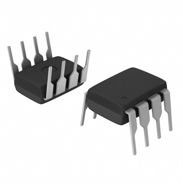
AT24C256-10PI EEPROM Memory IC Equivalent & Substitute Parts
Part Overview
The AT24C256-10PI is a 256Kbit I2C EEPROM memory IC manufactured by Microchip Technology, housed in an 8-DIP through-hole package. This device operates at 1 MHz clock frequency with 550 ns access time and supports supply voltages from 4.5V to 5.5V across an operating temperature range of -40°C to 85°C. The part is currently classified as obsolete, necessitating identification of functionally equivalent alternatives for new designs and ongoing system support.
Substiute Parts
Key Parameters
| Parameter | Value |
|---|---|
| Memory Size | 256Kbit |
| Memory Organization | 32K x 8 |
| Memory Interface | I2C |
| Clock Frequency | 1 MHz |
| Access Time | 550 ns |
| Write Cycle Time | 10 ms |
| Voltage Supply Range | 4.5V ~ 5.5V |
| Operating Temperature | -40°C ~ 85°C |
| Package Type | 8-DIP (0.300", 7.62mm) |
| Mounting Type | Through Hole |
Substitute Part Grouping Explanation
Substitution eligibility for the AT24C256-10PI is determined by the following critical parameters:
Primary Compatibility Criteria:
- Memory Interface: I2C protocol compatibility
- Package Type: 8-DIP form factor with 0.300" (7.62mm) pitch
- Mounting Type: Through-hole configuration
- Memory Organization: 32K x 8 or higher capacity
- Operating Temperature Range: Minimum -40°C ~ 85°C coverage
Secondary Compatibility Criteria:
- Supply Voltage Range: Must encompass or exceed 4.5V ~ 5.5V
- Clock Frequency: 1 MHz operation capability
- Access Time: 550 ns or faster performance
Two substitute parts meet these criteria with varying degrees of parameter alignment:
24AA256-I/P: Direct memory capacity match (256Kbit, 32K x 8) with identical package and interface. Operates at reduced clock frequency (400 kHz) and slower access time (900 ns), but supports wider supply voltage range (1.7V ~ 5.5V). Product status is active with RoHS3 compliance.
24FC515-I/P: Higher memory capacity (512Kbit, 64K x 8) with identical package and interface. Maintains 1 MHz clock frequency with improved access time (400 ns). Supports wider supply voltage range (2.5V ~ 5.5V). Product status is active with RoHS3 compliance.
Parameter Comparison
| Parameter | AT24C256-10PI (Main) | 24AA256-I/P | 24FC515-I/P |
|---|---|---|---|
| Memory Size | 256Kbit | 256Kbit | 512Kbit |
| Memory Organization | 32K x 8 | 32K x 8 | 64K x 8 |
| Memory Interface | I2C | I2C | I2C |
| Clock Frequency | 1 MHz | 400 kHz | 1 MHz |
| Access Time | 550 ns | 900 ns | 400 ns |
| Write Cycle Time | 10 ms | 5 ms | 5 ms |
| Voltage Supply Range | 4.5V ~ 5.5V | 1.7V ~ 5.5V | 2.5V ~ 5.5V |
| Operating Temperature | -40°C ~ 85°C | -40°C ~ 85°C | -40°C ~ 85°C |
| Package / Case | 8-DIP (0.300", 7.62mm) | 8-DIP (0.300", 7.62mm) | 8-DIP (0.300", 7.62mm) |
| Mounting Type | Through Hole | Through Hole | Through Hole |
| Product Status | Obsolete | Active | Active |
| RoHS Status | RoHS non-compliant | RoHS3 Compliant | RoHS3 Compliant |
Engineering Selection Recommendations
For Direct Replacement (Pin-Compatible, Functional Equivalence):
The 24AA256-I/P serves as the primary direct substitute for AT24C256-10PI applications. Both devices share identical memory capacity (256Kbit), organization (32K x 8), I2C interface, and 8-DIP package footprint. The 24AA256-I/P is currently in active production status with RoHS3 compliance certification, addressing the obsolescence of the original part. The reduced clock frequency (400 kHz versus 1 MHz) and slower access time (900 ns versus 550 ns) are acceptable for most legacy system implementations where timing margins exist. The extended supply voltage range (1.7V ~ 5.5V) provides additional design flexibility.
For Enhanced Performance or Expanded Capacity:
The 24FC515-I/P offers superior performance characteristics with maintained 1 MHz clock frequency and improved access time (400 ns). The doubled memory capacity (512Kbit, 64K x 8) accommodates applications requiring expanded storage without package or interface changes. This part is active production status with RoHS3 compliance. Selection of 24FC515-I/P is appropriate when system architecture permits address space utilization of the additional 256Kbit capacity or when faster access times provide system-level performance benefits.
Both substitute parts maintain identical operating temperature range (-40°C ~ 85°C) and through-hole mounting configuration, ensuring mechanical and thermal compatibility with existing PCB designs.
Frequently Asked Questions (FAQ)
Q: Can the 24AA256-I/P directly replace the AT24C256-10PI in existing designs?
A: Yes. Both devices use identical I2C protocol, 8-DIP package footprint, and 32K x 8 memory organization. Pin assignments are compatible. The 24AA256-I/P operates at reduced clock frequency (400 kHz) and slower access time (900 ns), which is acceptable for applications where the original 1 MHz / 550 ns specification included timing margin. Verify that your system timing does not require the original 1 MHz performance before substitution.
Q: What is the primary difference between 24AA256-I/P and 24FC515-I/P?
A: Memory capacity and access time differ. The 24AA256-I/P maintains 256Kbit capacity (32K x 8) with 900 ns access time at 400 kHz clock frequency. The 24FC515-I/P provides 512Kbit capacity (64K x 8) with 400 ns access time at 1 MHz clock frequency. Both use I2C interface and 8-DIP packaging. Selection depends on whether your application requires the additional storage capacity and whether faster access time provides system benefit.
Q: Are both substitute parts RoHS compliant?
A: Yes. Both 24AA256-I/P and 24FC515-I/P carry RoHS3 compliance certification. The original AT24C256-10PI is RoHS non-compliant. Substitution with either part satisfies RoHS compliance requirements for new designs and system updates.
Q: Will the 24FC515-I/P work in a circuit designed for AT24C256-10PI?
A: The 24FC515-I/P is pin-compatible and uses the same I2C protocol and 8-DIP package. However, the doubled memory capacity (512Kbit versus 256Kbit) requires that your system firmware or software can address the additional memory space. If your application firmware is hardcoded for 256Kbit addressing, the extra 256Kbit capacity will be inaccessible. Verify firmware compatibility before substitution.
Q: What supply voltage range should I use for substitution?
A: The original AT24C256-10PI requires 4.5V ~ 5.5V. The 24AA256-I/P supports 1.7V ~ 5.5V, and the 24FC515-I/P supports 2.5V ~ 5.5V. Both substitutes are compatible with the original 4.5V ~ 5.5V range. If your system operates at lower voltages (below 4.5V), only the 24AA256-I/P remains functional down to 1.7V.
Q: Are there any write cycle time differences I should consider?
A: Yes. The original AT24C256-10PI has a 10 ms write cycle time. Both substitutes (24AA256-I/P and 24FC515-I/P) have 5 ms write cycle time, which is faster. This improvement does not create compatibility issues; systems designed for 10 ms cycles will function correctly with 5 ms cycle devices.
Alternative Parts

SJ6012L2TP
Littelfuse Inc.
6 Alternative Parts

JMK107BBJ476MA-RE
Taiyo Yuden
10 Alternative Parts

GMK107BBJ475MA-T
Taiyo Yuden
5 Alternative Parts
SJ6020N2ARP
Littelfuse Inc.
3 Alternative Parts
SJ6025R2ATP
Littelfuse Inc.
4 Alternative Parts

2474-05L
API Delevan Inc.
1 Alternative Parts

4590R-684K
API Delevan Inc.
1 Alternative Parts

CM6560R-334
API Delevan Inc.
1 Alternative Parts

CM6460-104
API Delevan Inc.
1 Alternative Parts

5526-12
API Delevan Inc.
1 Alternative Parts