


Request Quote
(Ships tomorrow)
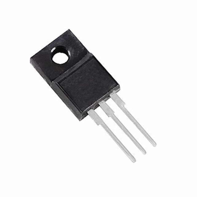
AOTF29S50L N-Channel 500V 29A MOSFET Equivalent & Substitute Parts
Part Overview
The AOTF29S50L is an N-Channel MOSFET manufactured by Alpha & Omega Semiconductor Inc., rated for 500V drain-to-source voltage with 29A continuous drain current at 25°C. This device is housed in a TO-220-3 Full Pack through-hole package and is designed for high-voltage switching applications. The part is currently in active production status with 2700 units in stock.
Equivalent and substitute parts are identified to provide design flexibility, accommodate supply chain variations, and support component sourcing alternatives while maintaining functional compatibility within specified electrical and mechanical parameters.
Substiute Parts
Key Parameters
| Parameter | Value | Unit |
|---|---|---|
| Drain to Source Voltage (Vdss) | 500 | V |
| Continuous Drain Current (Id) @ 25°C | 29 | A |
| Drive Voltage (Max Rds On) | 10 | V |
| Rds On (Max) @ Id, Vgs | 150 | mOhm |
| Gate Threshold Voltage (Vgs(th)) @ Id | 3.9 | V |
| Gate Charge (Qg) @ Vgs | 26.6 | nC |
| Maximum Gate Voltage (Vgs) | ±30 | V |
| Input Capacitance (Ciss) @ Vds | 1312 | pF |
| Power Dissipation (Max) | 37.9 | W |
| Operating Temperature Range | -55 to 150 | °C |
| Package Type | TO-220-3 Full Pack | Through Hole |
| FET Type | N-Channel | — |
| Technology | MOSFET (Metal Oxide) | — |
Substitute Part Grouping Explanation
Substitute parts for the AOTF29S50L are identified based on strict electrical and mechanical compatibility criteria. The primary substitution logic is based on the following parameters:
Critical Matching Parameters:
- Drain to Source Voltage (Vdss): 500V minimum
- FET Type: N-Channel
- Technology: MOSFET (Metal Oxide)
- Package Type: TO-220-3 Full Pack (through-hole mounting)
- Operating Temperature Range: Minimum -55°C to 150°C
Secondary Compatibility Parameters:
- Continuous Drain Current (Id): Rated at or above 21A
- On-State Resistance (Rds On): Within acceptable operating margins
- Gate Threshold Voltage (Vgs(th)): Within ±0.1V of specified value
- Maximum Gate Voltage (Vgs): ±25V or greater
The STF28NM50N from STMicroelectronics meets all critical matching parameters and operates within acceptable secondary parameter ranges, qualifying it as a direct substitute for the AOTF29S50L in applications where the specified electrical characteristics are required.
Parameter Comparison
| Parameter | AOTF29S50L (Alpha & Omega) | STF28NM50N (STMicroelectronics) | Unit |
|---|---|---|---|
| Drain to Source Voltage (Vdss) | 500 | 500 | V |
| Continuous Drain Current (Id) @ 25°C | 29 | 21 | A |
| Drive Voltage (Max Rds On) | 10 | 10 | V |
| Rds On (Max) @ Id, Vgs | 150 @ 14.5A, 10V | 158 @ 10.5A, 10V | mOhm |
| Gate Threshold Voltage (Vgs(th)) @ Id | 3.9 @ 250µA | 4.0 @ 250µA | V |
| Gate Charge (Qg) @ Vgs | 26.6 @ 10V | 50 @ 10V | nC |
| Maximum Gate Voltage (Vgs) | ±30 | ±25 | V |
| Input Capacitance (Ciss) @ Vds | 1312 @ 100V | 1735 @ 25V | pF |
| Power Dissipation (Max) | 37.9 | 35 | W |
| Operating Temperature Range | -55 to 150 | -55 to 150 | °C |
| Package Type | TO-220-3 Full Pack | TO-220-3 Full Pack | — |
| FET Type | N-Channel | N-Channel | — |
| Technology | MOSFET (Metal Oxide) | MOSFET (Metal Oxide) | — |
| RoHS Status | ROHS3 Compliant | ROHS3 Compliant | — |
| REACH Status | REACH Unaffected | REACH Unaffected | — |
Engineering Selection Recommendations
AOTF29S50L (Primary Selection)
The AOTF29S50L is the specified component for applications requiring 29A continuous drain current at 500V. This device is in active production status with established supply availability (2700 units in stock). The part carries ROHS3 compliance and REACH Unaffected status, meeting regulatory requirements for industrial and commercial applications. The aMOS™ series designation indicates optimized performance characteristics for the specified voltage and current ratings.
STF28NM50N (Substitute Selection)
The STF28NM50N qualifies as a functional substitute when the AOTF29S50L is unavailable. This device maintains identical voltage ratings (500V Vdss) and package configuration (TO-220-3 Full Pack). The STF28NM50N operates within the same temperature range (-55°C to 150°C) and carries equivalent regulatory compliance (ROHS3 Compliant, REACH Unaffected status).
Key Differences Affecting Application Suitability:
The STF28NM50N exhibits a reduced continuous drain current rating of 21A compared to the AOTF29S50L's 29A specification. Applications operating at or below 21A continuous current are fully compatible with the substitute. Applications requiring current levels between 21A and 29A require thermal analysis to confirm adequate heat dissipation, as the STF28NM50N has a maximum power dissipation of 35W versus the AOTF29S50L's 37.9W.
The STF28NM50N exhibits higher gate charge (50 nC versus 26.6 nC) and input capacitance (1735 pF versus 1312 pF), resulting in increased switching losses and slower switching response. Gate drive circuits must be evaluated for compatibility with these increased capacitive loads.
Both devices are suitable for direct pin-compatible replacement in TO-220-3 Full Pack footprints without PCB modification.
Frequently Asked Questions (FAQ)
Q: Can the STF28NM50N directly replace the AOTF29S50L in all applications?
A: Direct replacement is possible for applications operating at continuous drain currents of 21A or below. Applications requiring the full 29A rating of the AOTF29S50L require current derating or thermal management modifications when using the STF28NM50N.
Q: What are the package compatibility considerations?
A: Both the AOTF29S50L and STF28NM50N use identical TO-220-3 Full Pack through-hole packages. Pin assignments are compatible, and no PCB modifications are required for physical replacement. Thermal interface materials and heatsink mounting remain unchanged.
Q: How do the gate charge differences affect circuit design?
A: The STF28NM50N exhibits 88% higher gate charge (50 nC versus 26.6 nC). Gate drive circuits must supply sufficient current to charge the gate within the required switching time. High-frequency switching applications may experience increased switching losses due to the higher gate charge requirement.
Q: Are there regulatory or compliance differences between these parts?
A: Both devices carry identical regulatory status: ROHS3 Compliant and REACH Unaffected. No compliance modifications are required when substituting between these parts.
Q: What thermal considerations apply to substitution?
A: The STF28NM50N has a maximum power dissipation of 35W compared to the AOTF29S50L's 37.9W. For applications operating near maximum power dissipation limits, verify that thermal management (heatsink sizing, thermal interface materials) remains adequate with the substitute device.
Q: How do the on-state resistance specifications compare?
A: The AOTF29S50L specifies 150 mOhm at 14.5A and 10V gate voltage. The STF28NM50N specifies 158 mOhm at 10.5A and 10V gate voltage. The STF28NM50N exhibits slightly higher on-state resistance, resulting in marginally increased conduction losses at equivalent current levels.
Q: Are there voltage rating differences?
A: Both devices are rated for 500V drain-to-source voltage. The AOTF29S50L permits ±30V gate voltage, while the STF28NM50N permits ±25V gate voltage. Gate drive circuits must operate within the ±25V limit when using the STF28NM50N.
Q: What is the operating temperature compatibility?
A: Both devices operate across the identical temperature range of -55°C to 150°C junction temperature. No thermal operating range modifications are required for substitution.
Alternative Parts

SJ6012L2TP
Littelfuse Inc.
6 Alternative Parts

JMK107BBJ476MA-RE
Taiyo Yuden
10 Alternative Parts

GMK107BBJ475MA-T
Taiyo Yuden
5 Alternative Parts
SJ6020N2ARP
Littelfuse Inc.
3 Alternative Parts
SJ6025R2ATP
Littelfuse Inc.
4 Alternative Parts

2474-05L
API Delevan Inc.
1 Alternative Parts

4590R-684K
API Delevan Inc.
1 Alternative Parts

CM6560R-334
API Delevan Inc.
1 Alternative Parts

CM6460-104
API Delevan Inc.
1 Alternative Parts

5526-12
API Delevan Inc.
1 Alternative Parts