


Request Quote
(Ships tomorrow)
AOTF262L N-Channel MOSFET 60V 17.5A/85A TO-220 Equivalent & Substitute Parts
Part Overview
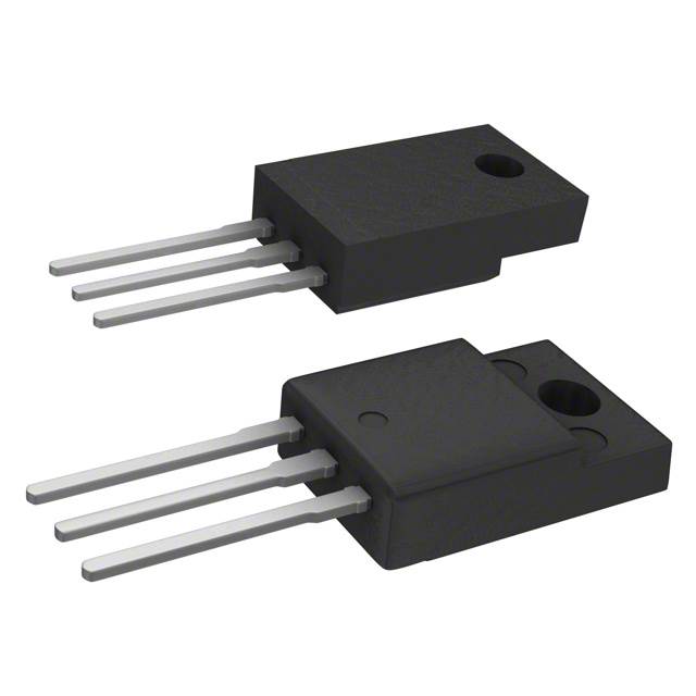
The AOTF262L is an N-Channel MOSFET manufactured by Alpha & Omega Semiconductor Inc., rated for 60V drain-to-source voltage with continuous drain current of 17.5A at Ta (ambient temperature) or 85A at Tc (case temperature). The device is housed in a TO-220-3 Full Pack through-hole package and is designed for general-purpose switching and amplification applications requiring moderate to high current handling in a standard thermal package.
The AOTF262L is classified as obsolete. Locating equivalent or substitute components becomes necessary when original inventory is depleted, when procurement lead times are extended, or when design flexibility is required for new production runs. Substitute parts must maintain electrical compatibility across critical parameters including drain-to-source voltage rating, continuous drain current capability, on-resistance characteristics, and gate threshold voltage to ensure functional equivalence in the target application.
Substiute Parts
Key Parameters
| Parameter | Value | Unit | Condition |
|---|---|---|---|
| Drain to Source Voltage (Vdss) | 60 | V | Maximum rating |
| Current - Continuous Drain (Id) @ 25°C | 17.5 (Ta) / 85 (Tc) | A | Ambient / Case temperature |
| Rds On (Max) @ Id, Vgs | 3.6 | mOhm | @ 20A, 10V |
| Vgs(th) (Max) @ Id | 3.2 | V | @ 250µA |
| Gate Charge (Qg) (Max) @ Vgs | 135 | nC | @ 10V |
| Vgs (Max) | ±20 | V | Gate-source voltage rating |
| Input Capacitance (Ciss) (Max) @ Vds | 8140 | pF | @ 30V |
| Power Dissipation (Max) | 2.1 (Ta) / 50 (Tc) | W | Ambient / Case temperature |
| Operating Temperature | -55 to 175 | °C | Junction temperature (TJ) |
| Mounting Type | Through Hole | - | TO-220-3 Full Pack |
| FET Type | N-Channel | - | MOSFET (Metal Oxide) |
Substitute Part Grouping Explanation
Substitution of the AOTF262L is determined by strict electrical and mechanical compatibility across the following critical parameters:
Voltage Rating Compatibility: All substitute parts must maintain a Drain-to-Source Voltage (Vdss) rating of 60V or greater to ensure the device can safely operate in circuits designed for the AOTF262L.
Current Handling Capability: Substitute parts must support continuous drain current (Id) at case temperature (Tc) equal to or exceeding the AOTF262L specification of 85A (Tc). This ensures the substitute can handle the same thermal load and current demands.
On-Resistance (Rds On): The on-resistance at specified gate-source voltage (Vgs) and drain current (Id) must be equal to or lower than the AOTF262L specification of 3.6 mOhm @ 20A, 10V. Lower on-resistance reduces power dissipation and heat generation in the application.
Gate Threshold Voltage (Vgs(th)): The gate threshold voltage must be compatible with the AOTF262L specification of 3.2V @ 250µA to ensure proper gate drive compatibility and switching behavior.
Gate Charge (Qg): Gate charge characteristics must be within acceptable range to maintain switching speed and drive circuit compatibility.
Package and Mounting: All substitute parts must use through-hole TO-220 package variants (TO-220F, TO-220FP, TO-220SIS) to ensure mechanical and thermal interface compatibility with existing PCB designs.
Temperature Range: Operating temperature range must encompass or match the AOTF262L range of -55°C to 175°C (TJ).
Parameter Comparison
| Parameter | AOTF262L (Alpha & Omega) | STF40NF06 (STMicroelectronics) | TK100A06N1,S4X (Toshiba) | Unit | Condition |
|---|---|---|---|---|---|
| Drain to Source Voltage (Vdss) | 60 | 60 | 60 | V | Maximum rating |
| Current - Continuous Drain (Id) @ 25°C | 17.5 (Ta) / 85 (Tc) | 23 (Tc) | 100 (Tc) | A | Ambient / Case temperature |
| Rds On (Max) @ Id, Vgs | 3.6 @ 20A, 10V | 28 @ 11.5A, 10V | 2.7 @ 50A, 10V | mOhm | Specified conditions |
| Vgs(th) (Max) @ Id | 3.2 @ 250µA | 4 @ 250µA | 4 @ 1mA | V | Gate threshold voltage |
| Gate Charge (Qg) (Max) @ Vgs | 135 @ 10V | 32 @ 10V | 140 @ 10V | nC | @ 10V gate-source voltage |
| Vgs (Max) | ±20 | ±20 | ±20 | V | Gate-source voltage rating |
| Input Capacitance (Ciss) (Max) @ Vds | 8140 @ 30V | 920 @ 25V | 10500 @ 30V | pF | Specified drain-source voltage |
| Power Dissipation (Max) | 2.1 (Ta) / 50 (Tc) | 30 (Tc) | 45 (Tc) | W | Ambient / Case temperature |
| Operating Temperature | -55 to 175 | -55 to 175 | -55 to 150 | °C | Junction temperature (TJ) |
| Mounting Type | Through Hole | Through Hole | Through Hole | - | Package type |
| Package / Case | TO-220-3 Full Pack | TO-220-3 Full Pack | TO-220-3 Full Pack | - | Physical package |
Engineering Selection Recommendations
STF40NF06 (STMicroelectronics): This substitute meets the 60V Vdss requirement and provides 23A continuous drain current at case temperature. The device is RoHS3 compliant and carries REACH Unaffected status, meeting modern environmental and regulatory requirements. The STF40NF06 is classified as obsolete, matching the product status of the AOTF262L. The on-resistance of 28 mOhm @ 11.5A, 10V is higher than the AOTF262L specification, indicating increased power dissipation in high-current applications. This substitute is suitable for applications where current requirements do not exceed 23A continuous operation.
TK100A06N1,S4X (Toshiba Semiconductor and Storage): This substitute exceeds the AOTF262L specifications across multiple parameters. It provides 100A continuous drain current at case temperature, significantly higher than the AOTF262L's 85A rating. The on-resistance of 2.7 mOhm @ 50A, 10V is superior to the AOTF262L specification of 3.6 mOhm, resulting in lower power dissipation and improved thermal performance. The TK100A06N1,S4X is classified as Active product status, indicating ongoing manufacturer support and availability. RoHS3 compliance and REACH Unaffected status confirm regulatory alignment. The operating temperature range extends to 150°C (TJ), which is 25°C lower than the AOTF262L maximum of 175°C. This substitute is suitable for applications requiring higher current capacity, lower on-resistance, and long-term component availability.
Selection Basis: Both substitutes maintain the critical 60V Vdss rating and through-hole TO-220 package compatibility. The choice between STF40NF06 and TK100A06N1,S4X depends on application current requirements and thermal management strategy. The Toshiba device provides superior electrical performance and active product status, making it the preferred choice for new designs or applications requiring extended component lifecycle support.
Frequently Asked Questions (FAQ)
Q: Can the STF40NF06 be used as a direct replacement for the AOTF262L in all applications?
A: The STF40NF06 maintains voltage rating and package compatibility but provides lower continuous drain current (23A vs. 85A at Tc) and higher on-resistance (28 mOhm vs. 3.6 mOhm). It is suitable only for applications where continuous drain current does not exceed 23A. Verify application current requirements before substitution.
Q: What are the advantages of using the TK100A06N1,S4X over the AOTF262L?
A: The TK100A06N1,S4X provides higher continuous drain current (100A vs. 85A at Tc), lower on-resistance (2.7 mOhm vs. 3.6 mOhm), and active product status with ongoing manufacturer support. These characteristics result in improved thermal performance and extended component availability.
Q: Are all three devices pin-compatible?
A: All three devices use TO-220-3 Full Pack through-hole packages with identical pin configurations (Gate, Drain, Source). Physical PCB layout compatibility is maintained across all three parts.
Q: What is the impact of higher on-resistance in the STF40NF06 substitute?
A: Higher on-resistance increases power dissipation during conduction. In applications with continuous high current operation, the STF40NF06 will generate more heat than the AOTF262L. Thermal management and heat sink design must account for this increased dissipation.
Q: Does the lower maximum operating temperature of the TK100A06N1,S4X (150°C vs. 175°C) limit its use?
A: The TK100A06N1,S4X maximum junction temperature of 150°C is lower than the AOTF262L specification of 175°C. For applications operating near the upper temperature limit, verify that the TK100A06N1,S4X thermal design accommodates the 25°C reduction in maximum allowable junction temperature.
Q: Are there compliance or regulatory differences between the three devices?
A: The STF40NF06 and TK100A06N1,S4X are both RoHS3 compliant and REACH Unaffected. The AOTF262L compliance status is not specified in the provided data. Both substitutes meet modern environmental and regulatory requirements for electronic component procurement.
Q: What is the significance of the TK100A06N1,S4X being classified as Active product status?
A: Active product status indicates that Toshiba continues to manufacture and support this component. This ensures ongoing availability, stable pricing, and access to technical documentation. The AOTF262L and STF40NF06 are both obsolete, meaning manufacturer support and availability may be limited.
Q: How do gate charge differences affect circuit design?
A: The STF40NF06 has significantly lower gate charge (32 nC vs. 135 nC for AOTF262L), requiring less gate drive energy and enabling faster switching. The TK100A06N1,S4X gate charge (140 nC) is comparable to the AOTF262L. Gate drive circuits must be verified to ensure adequate charge delivery for proper switching performance.
Alternative Parts

SJ6012L2TP
Littelfuse Inc.
6 Alternative Parts

JMK107BBJ476MA-RE
Taiyo Yuden
10 Alternative Parts

GMK107BBJ475MA-T
Taiyo Yuden
5 Alternative Parts
SJ6020N2ARP
Littelfuse Inc.
3 Alternative Parts
SJ6025R2ATP
Littelfuse Inc.
4 Alternative Parts

2474-05L
API Delevan Inc.
1 Alternative Parts

4590R-684K
API Delevan Inc.
1 Alternative Parts

CM6560R-334
API Delevan Inc.
1 Alternative Parts

CM6460-104
API Delevan Inc.
1 Alternative Parts

5526-12
API Delevan Inc.
1 Alternative Parts