


Request Quote
(Ships tomorrow)
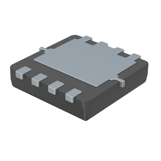
AON7442 N-Channel MOSFET 30V 50A Equivalent & Substitute Parts
Part Overview
The AON7442 is an N-Channel enhancement mode MOSFET manufactured by Alpha & Omega Semiconductor Inc., rated for 30V drain-to-source voltage with 50A continuous drain current at 25°C. The device is housed in an 8-DFN-EP (3.3x3.3) surface mount package and dissipates up to 83W at the case temperature. This part is classified as "Not For New Designs," indicating it has been superseded or is in end-of-life status. Identifying equivalent substitute parts is necessary for ongoing production support, maintenance applications, and design continuity where the AON7442 specification requirements must be maintained.
Substiute Parts
Key Parameters
| Parameter | Value | Unit |
|---|---|---|
| Drain-to-Source Voltage (Vdss) | 30 | V |
| Continuous Drain Current (Id) @ 25°C | 50 | A (Tc) |
| On-Resistance (Rds On Max) @ Id, Vgs | 1.9 | mOhm @ 20A, 10V |
| Gate Threshold Voltage (Vgs(th) Max) @ Id | 2.2 | V @ 250µA |
| Power Dissipation (Max) | 83 | W (Tc) |
| Operating Temperature Range | -55 to 150 | °C (TJ) |
| Package Type | 8-DFN-EP (3.3x3.3) | Surface Mount |
| RoHS Status | ROHS3 Compliant | - |
| Moisture Sensitivity Level | 1 (Unlimited) | - |
Substitute Part Grouping Explanation
Substitution of the AON7442 is determined by electrical and mechanical compatibility across the following critical parameters:
Electrical Compatibility Criteria:
- Drain-to-Source Voltage (Vdss) must equal or exceed 30V
- Continuous Drain Current (Id) must support the application's current requirements
- On-Resistance (Rds On) characteristics must be compatible with thermal and efficiency constraints
- Gate Threshold Voltage (Vgs(th)) must fall within acceptable switching characteristics
- Operating temperature range must encompass -55°C to 150°C (TJ)
Mechanical Compatibility Criteria:
- Surface mount package configuration
- Pin count and footprint compatibility with 8-pin DFN format
- Thermal performance (power dissipation capability)
Compliance Criteria:
- RoHS3 compliance status
- Moisture Sensitivity Level (MSL) rating
- REACH and ECCN classifications
The PJQ4402P_R2_00001 meets the core voltage and package requirements. However, differences in continuous drain current rating and on-resistance characteristics must be evaluated against specific application demands.
Parameter Comparison
| Parameter | AON7442 | PJQ4402P_R2_00001 | Unit |
|---|---|---|---|
| Manufacturer | Alpha & Omega Semiconductor Inc. | Panjit International Inc. | - |
| FET Type | N-Channel | N-Channel | - |
| Drain-to-Source Voltage (Vdss) | 30 | 30 | V |
| Continuous Drain Current (Id) @ 25°C | 50 (Tc) | 70 (Tc) | A |
| On-Resistance (Rds On Max) @ Id, Vgs | 1.9 @ 20A, 10V | 3.8 @ 10A, 10V | mOhm |
| Gate Threshold Voltage (Vgs(th) Max) @ Id | 2.2 @ 250µA | 2.5 @ 250µA | V |
| Gate Charge (Qg) Max @ Vgs | 65 @ 10V | 23 @ 4.5V | nC |
| Input Capacitance (Ciss) Max @ Vds | 2994 @ 15V | 2436 @ 25V | pF |
| Power Dissipation (Max) | 83 (Tc) | 39 (Tc) | W |
| Operating Temperature Range | -55 to 150 | -55 to 150 | °C (TJ) |
| Package Type | 8-DFN-EP (3.3x3.3) | DFN3333-8 | Surface Mount |
| Product Status | Not For New Designs | Active | - |
| RoHS Status | ROHS3 Compliant | ROHS3 Compliant | - |
| Moisture Sensitivity Level | 1 (Unlimited) | 1 (Unlimited) | - |
Engineering Selection Recommendations
Product Status Consideration: The AON7442 carries a "Not For New Designs" designation, while the PJQ4402P_R2_00001 maintains "Active" status. For applications requiring long-term component availability and manufacturer support, the PJQ4402P_R2_00001 is the preferred choice.
Compliance Alignment: Both parts are ROHS3 compliant, carry MSL Level 1 (Unlimited) moisture sensitivity ratings, and share identical REACH and ECCN classifications (EAR99 and 8541.29.0095 respectively). No compliance barriers exist for substitution.
Electrical Performance Trade-offs: The PJQ4402P_R2_00001 provides higher continuous drain current capability (70A Tc versus 50A Tc) but exhibits higher on-resistance (3.8 mOhm @ 10A, 10V versus 1.9 mOhm @ 20A, 10V). The substitute part also demonstrates lower power dissipation rating (39W Tc versus 83W Tc) and reduced gate charge (23 nC @ 4.5V versus 65 nC @ 10V).
Package Compatibility: Both devices employ 8-pin DFN surface mount packages with identical 3.3x3.3mm footprints. Physical board-level compatibility is established.
Application-Specific Evaluation: Selection between these parts depends on the specific application's current and thermal requirements. Applications operating at or near the AON7442's 50A rating may require thermal analysis when transitioning to the PJQ4402P_R2_00001 due to its lower power dissipation specification.
Frequently Asked Questions (FAQ)
Q: Can the PJQ4402P_R2_00001 directly replace the AON7442 in existing designs?
A: Direct replacement is possible from a package and voltage standpoint. Both parts share identical 30V Vdss ratings, 8-pin DFN surface mount packages, and operating temperature ranges. However, differences in on-resistance, gate charge, and power dissipation specifications require application-level verification. Designs operating at the AON7442's maximum current or thermal limits may require circuit adjustments.
Q: What are the key electrical differences between these parts?
A: The AON7442 offers lower on-resistance (1.9 mOhm @ 20A, 10V) and higher power dissipation capability (83W Tc), making it suitable for high-current, high-power applications. The PJQ4402P_R2_00001 provides higher drain current rating (70A Tc) but with higher on-resistance (3.8 mOhm @ 10A, 10V) and lower power dissipation (39W Tc). Gate charge is significantly lower in the substitute (23 nC @ 4.5V versus 65 nC @ 10V), affecting switching speed characteristics.
Q: Are the package footprints identical?
A: Both parts use 8-pin DFN packages with 3.3x3.3mm dimensions. The AON7442 is specified as 8-DFN-EP, while the PJQ4402P_R2_00001 is specified as DFN3333-8. These designations refer to the same physical footprint standard, ensuring PCB-level compatibility.
Q: What is the significance of the AON7442's "Not For New Designs" status?
A: This designation indicates the part has reached end-of-life or has been superseded by the manufacturer. While existing inventory may be available, Alpha & Omega Semiconductor Inc. does not recommend this part for new product development. The PJQ4402P_R2_00001, with "Active" status, represents the current-generation alternative with ongoing manufacturer support.
Q: Do both parts meet the same compliance standards?
A: Yes. Both the AON7442 and PJQ4402P_R2_00001 are ROHS3 compliant, carry MSL Level 1 ratings, and share identical REACH and ECCN classifications. No compliance barriers exist for substitution in regulated applications.
Q: How do gate charge differences affect circuit design?
A: The PJQ4402P_R2_00001 exhibits significantly lower gate charge (23 nC @ 4.5V) compared to the AON7442 (65 nC @ 10V). Lower gate charge enables faster switching transitions and reduces gate driver power requirements. Applications with tight switching frequency constraints or high-frequency operation may benefit from this characteristic.
Q: Which part should be selected for new production?
A: The PJQ4402P_R2_00001 is the appropriate choice for new production due to its "Active" product status, ensuring long-term availability and manufacturer support. The AON7442 should be reserved for legacy system maintenance where the original specification is mandatory.
Alternative Parts

SJ6012L2TP
Littelfuse Inc.
6 Alternative Parts

JMK107BBJ476MA-RE
Taiyo Yuden
10 Alternative Parts

GMK107BBJ475MA-T
Taiyo Yuden
5 Alternative Parts
SJ6020N2ARP
Littelfuse Inc.
3 Alternative Parts
SJ6025R2ATP
Littelfuse Inc.
4 Alternative Parts

2474-05L
API Delevan Inc.
1 Alternative Parts

4590R-684K
API Delevan Inc.
1 Alternative Parts

CM6560R-334
API Delevan Inc.
1 Alternative Parts

CM6460-104
API Delevan Inc.
1 Alternative Parts

5526-12
API Delevan Inc.
1 Alternative Parts