


Request Quote
(Ships tomorrow)
AON6444 Equivalent & Substitute Parts
Part Overview
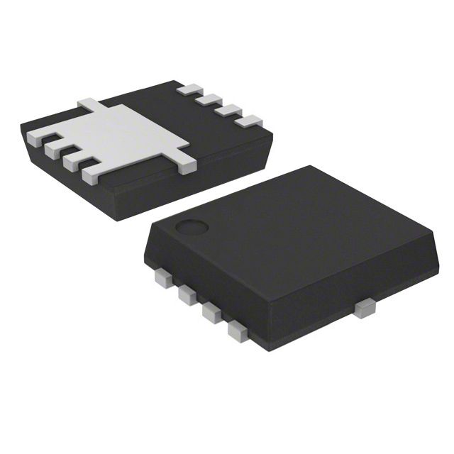
The AON6444 is an N-Channel 60V MOSFET manufactured by Alpha & Omega Semiconductor Inc., designed for surface mount applications in the 8-DFN (5x6) package. This device operates as part of the SDMOS™ series and is rated for continuous drain current of 14A at Ta and 81A at Tc, with maximum power dissipation of 2.3W (Ta) and 83W (Tc). The AON6444 is classified as obsolete, making equivalent and substitute parts necessary for new designs and ongoing production requirements. Substitute parts must maintain compatibility across critical electrical parameters including drain-source voltage, gate threshold voltage, and thermal characteristics while accommodating different package formats and manufacturer technologies.
Substiute Parts
Key Parameters
| Parameter | AON6444 Value | Unit |
|---|---|---|
| Drain to Source Voltage (Vdss) | 60 | V |
| Continuous Drain Current @ 25°C (Ta) | 14 | A |
| Continuous Drain Current @ 25°C (Tc) | 81 | A |
| Rds On (Max) @ 20A, 10V | 6.5 | mOhm |
| Gate Threshold Voltage (Vgs(th)) @ 250µA | 2.5 | V |
| Gate Charge (Qg) @ 10V | 96 | nC |
| Input Capacitance (Ciss) @ 30V | 5800 | pF |
| Operating Temperature Range | -55 to 150 | °C |
| Package Type | 8-DFN (5x6) | - |
| FET Type | N-Channel | - |
| Technology | MOSFET (Metal Oxide) | - |
| Product Status | Obsolete | - |
Substitute Part Grouping Explanation
Substitute parts for the AON6444 are selected based on strict electrical and mechanical compatibility criteria. All substitute devices maintain the following critical parameters:
Mandatory Compatibility Parameters:
- Drain to Source Voltage (Vdss): 60V
- FET Type: N-Channel
- Technology: MOSFET (Metal Oxide)
- Gate Threshold Voltage (Vgs(th)): 2.0V to 4.0V @ 250µA to 300µA
- Maximum Gate Voltage (Vgs): ±20V
- Operating Temperature Range: -55°C to 150°C
- Mounting Type: Surface Mount
- Moisture Sensitivity Level: 1 (Unlimited)
Substitution Logic:
Substitute parts are grouped into two categories based on package compatibility and current rating characteristics:
Category 1 - Direct Package Compatibility (8-DFN/8-VSON/8-PowerSMD variants): AON6268, CSD18533Q5A, CSD18533Q5AT, and CSD18563Q5AT maintain similar footprint dimensions (5x6mm) with enhanced electrical performance. These devices offer improved gate charge characteristics and reduced input capacitance compared to the AON6444, enabling faster switching and lower drive requirements.
Category 2 - Alternative Package Formats (8-SOP, 8-TSON, PowerDI3333): DMT6010LFG-13, TPH5R906NH,L1Q, and TPN7R506NH,L1Q provide functional equivalence with different package geometries. These alternatives accommodate design flexibility when board layout constraints or thermal management requirements necessitate alternative form factors.
All substitute parts are active products with current manufacturing status, ensuring long-term availability and supply chain stability.
Parameter Comparison
| Parameter | AON6444 | AON6268 | CSD18533Q5A | CSD18533Q5AT | CSD18563Q5AT | DMT6010LFG-13 | TPH5R906NH,L1Q | TPN7R506NH,L1Q |
|---|---|---|---|---|---|---|---|---|
| Vdss (V) | 60 | 60 | 60 | 60 | 60 | 60 | 60 | 60 |
| Id @ Ta (A) | 14 | - | 17 | 17 | 100 | 13 | 28 | - |
| Id @ Tc (A) | 81 | 44 | 100 | 100 | - | 30 | - | 26 |
| Rds On (Max) @ 10V (mOhm) | 6.5 | 4.7 | 5.9 | 5.9 | 6.8 | 7.5 | 5.9 | 7.5 |
| Vgs(th) @ 250µA (V) | 2.5 | 2.3 | 2.3 | 2.3 | 2.4 | 2.0 | 4.0 | 4.0 |
| Qg @ 10V (nC) | 96 | 65 | 36 | 36 | 20 | 41.3 | 38 | 22 |
| Ciss @ 30V (pF) | 5800 | 2520 | 2750 | 2750 | 1500 | 2090 | 3100 | 1800 |
| Vgs (Max) (V) | ±20 | ±20 | ±20 | ±20 | ±20 | ±20 | ±20 | ±20 |
| Operating Temp Range (°C) | -55 to 150 | -55 to 150 | -55 to 150 | -55 to 150 | -55 to 150 | -55 to 150 | -55 to 150 | -55 to 150 |
| Package | 8-DFN (5x6) | 8-DFN (5x6) | 8-VSONP (5x6) | 8-VSONP (5x6) | 8-VSONP (5x6) | PowerDI3333-8 | 8-SOP Advance (5x5) | 8-TSON Advance (3.1x3.1) |
| FET Type | N-Channel | N-Channel | N-Channel | N-Channel | N-Channel | N-Channel | N-Channel | N-Channel |
| Technology | MOSFET | MOSFET | MOSFET | MOSFET | MOSFET | MOSFET | MOSFET | MOSFET |
| Product Status | Obsolete | Active | Active | Active | Active | Active | Active | Active |
| RoHS Status | REACH Unaffected | ROHS3 Compliant | ROHS3 Compliant | ROHS3 Compliant | ROHS3 Compliant | ROHS3 Compliant | RoHS Compliant | RoHS Compliant |
Engineering Selection Recommendations
For Direct Package Replacement (Recommended for PCB Compatibility):
AON6268 provides the closest form factor match to the AON6444 within the 8-DFN (5x6) package family. This device is manufactured by Alpha & Omega Semiconductor Inc., maintaining design continuity with the original part. AON6268 is ROHS3 compliant and carries active product status with substantial inventory availability (17,175 pcs). The reduced gate charge (65 nC vs. 96 nC) and lower input capacitance (2520 pF vs. 5800 pF) enable improved switching performance in existing circuit topologies.
For Enhanced Performance with Package Flexibility:
CSD18533Q5AT and CSD18533Q5A (Texas Instruments NexFET™ series) offer superior electrical characteristics with significantly reduced gate charge (36 nC) and input capacitance (2750 pF). These devices are ROHS3 compliant and maintain active product status with high inventory levels (6,900 and 52,800 pcs respectively). The 8-VSONP (5x6) package provides mechanical compatibility with similar footprint dimensions to the original 8-DFN package.
CSD18563Q5AT delivers the lowest gate charge (20 nC) and input capacitance (1500 pF) among all substitutes, enabling fastest switching transitions. This device is ROHS3 compliant with active status and 47,019 pcs in stock.
For Alternative Package Geometries:
DMT6010LFG-13 (Diodes Incorporated) accommodates designs requiring the PowerDI3333-8 package format. This device is ROHS3 compliant with active status and 9,269 pcs available.
TPH5R906NH,L1Q and TPN7R506NH,L1Q (Toshiba Semiconductor U-MOSVIII-H series) provide alternatives in 8-SOP Advance and 8-TSON Advance packages respectively. Both devices are RoHS compliant with active product status. TPN7R506NH,L1Q offers the most compact footprint (3.1x3.1mm) for space-constrained applications.
Compliance Considerations:
All substitute parts maintain REACH Unaffected or ROHS3 Compliant status, ensuring regulatory compliance across global markets. Moisture Sensitivity Level 1 (Unlimited) is consistent across all devices, eliminating moisture handling requirement changes during substitution.
Frequently Asked Questions (FAQ)
Q: Can AON6268 be used as a direct replacement for AON6444 without PCB modifications?
A: AON6268 shares the identical 8-DFN (5x6) package footprint with AON6444, enabling direct PCB placement without layout changes. Both devices use 8-PowerSMD flat lead configurations. Electrical parameter differences (lower Rds On, reduced gate charge, lower input capacitance) represent performance improvements compatible with existing circuit designs.
Q: What are the key differences between the CSD18533Q5A and CSD18533Q5AT variants?
A: CSD18533Q5A and CSD18533Q5AT are electrically identical N-Channel 60V MOSFETs with 17A (Ta) and 100A (Tc) continuous drain current ratings. The primary distinction is packaging format: CSD18533Q5A is supplied in Cut Tape (CT) & Digi-Reel® configuration, while CSD18533Q5AT is supplied in Tape & Reel (TR) format. Both use the 8-VSONP (5x6) package and are ROHS3 compliant with active product status.
Q: How does the CSD18563Q5AT compare to CSD18533Q5AT in terms of switching performance?
A: CSD18563Q5AT exhibits superior switching characteristics with gate charge of 20 nC compared to CSD18533Q5AT's 36 nC, and input capacitance of 1500 pF versus 2750 pF. These reductions enable faster switching transitions and lower gate drive power requirements. Both devices maintain 60V Vdss rating and ±20V maximum gate voltage. CSD18563Q5AT is rated for 100A continuous drain current at Ta, while CSD18533Q5AT is rated for 17A (Ta) and 100A (Tc).
Q: Are the Toshiba devices (TPH5R906NH,L1Q and TPN7R506NH,L1Q) suitable for high-frequency switching applications?
A: Both Toshiba devices support high-frequency operation. TPH5R906NH,L1Q features gate charge of 38 nC and input capacitance of 3100 pF in the 8-SOP Advance (5x5) package. TPN7R506NH,L1Q offers lower gate charge (22 nC) and input capacitance (1800 pF) in the compact 8-TSON Advance (3.1x3.1) package. The reduced parasitic capacitance of TPN7R506NH,L1Q makes it preferable for applications requiring minimal switching losses.
Q: What is the significance of the different gate threshold voltage specifications across substitute parts?
A: Gate threshold voltage (Vgs(th)) specifications range from 2.0V to 4.0V across the substitute parts. AON6444, AON6268, CSD18533Q5A, CSD18533Q5AT, and CSD18563Q5AT cluster around 2.3-2.5V, indicating compatibility with low-voltage gate drive circuits. DMT6010LFG-13 specifies 2.0V, while Toshiba devices (TPH5R906NH,L1Q and TPN7R506NH,L1Q) specify 4.0V. Higher threshold voltages require proportionally higher gate drive voltages for full device enhancement. Circuit designs must accommodate these differences in gate drive voltage levels.
Q: Can DMT6010LFG-13 be used in applications where thermal management is critical?
A: DMT6010LFG-13 is rated for 2.2W (Ta) and 41W (Tc) maximum power dissipation, lower than AON6444's 2.3W (Ta) and 83W (Tc). The PowerDI3333-8 package provides adequate thermal performance for moderate power applications. For designs requiring the thermal performance of AON6444 or higher, CSD18533Q5AT (116W Tc), CSD18563Q5AT (116W Tc), or AON6268 (56W Tc) are more suitable selections.
Q: What packaging considerations apply when substituting from 8-DFN to 8-VSONP format?
A: Both 8-DFN and 8-VSONP packages maintain 5x6mm footprint dimensions and 8-pin configurations with flat lead designs. The primary difference is internal die attachment and thermal path architecture. 8-VSONP packages typically offer enhanced thermal performance through optimized lead frame design. PCB layout compatibility is maintained, though thermal via placement and copper area distribution may require optimization to fully utilize the improved thermal characteristics of 8-VSONP devices.
Q: Are all substitute parts suitable for automotive applications?
A: All substitute parts listed maintain -55°C to 150°C operating temperature ranges and REACH/RoHS compliance status consistent with automotive qualification requirements. However, automotive applications typically require additional qualification documentation including AEC-Q101 certification. Specific automotive suitability must be confirmed through manufacturer datasheets and application notes beyond the parameters provided in this reference.
Q: What is the impact of reduced input capacitance on circuit design?
A: Reduced input capacitance (Ciss) directly decreases gate charge requirements and switching losses. CSD18563Q5AT's 1500 pF input capacitance (versus AON6444's 5800 pF) reduces gate drive power consumption and enables faster switching transitions. Lower input capacitance also reduces electromagnetic interference (EMI) generation during switching events. Circuit designs benefit from these reductions without requiring topology modifications, though gate drive circuits may be optimized for improved efficiency.
Alternative Parts

SJ6012L2TP
Littelfuse Inc.
6 Alternative Parts

JMK107BBJ476MA-RE
Taiyo Yuden
10 Alternative Parts

GMK107BBJ475MA-T
Taiyo Yuden
5 Alternative Parts
SJ6020N2ARP
Littelfuse Inc.
3 Alternative Parts
SJ6025R2ATP
Littelfuse Inc.
4 Alternative Parts

2474-05L
API Delevan Inc.
1 Alternative Parts

4590R-684K
API Delevan Inc.
1 Alternative Parts

CM6560R-334
API Delevan Inc.
1 Alternative Parts

CM6460-104
API Delevan Inc.
1 Alternative Parts

5526-12
API Delevan Inc.
1 Alternative Parts