


Request Quote
(Ships tomorrow)
AOD468 Equivalent & Substitute Parts
Part Overview
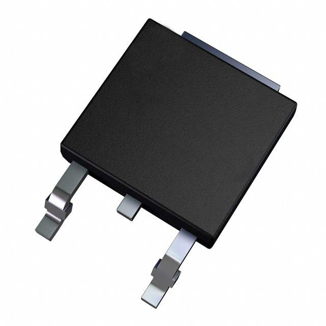
The AOD468 is an N-Channel MOSFET manufactured by Alpha & Omega Semiconductor Inc., rated for 300V drain-to-source voltage with 11.5A continuous drain current at 25°C. The device is housed in a TO-252 (DPAK) surface mount package and is designed for applications requiring moderate to high current switching at elevated voltage levels. The part is currently in active production status with RoHS3 compliance and unlimited moisture sensitivity level (MSL 1).
Substitute parts are identified when equivalent electrical performance can be achieved within the specified parameter ranges while maintaining package compatibility and compliance certifications. The AOD468 has two manufacturer-recommended substitutes that provide functional equivalence under specific application conditions.
Substiute Parts
Key Parameters
| Parameter | Value | Unit |
|---|---|---|
| Drain-to-Source Voltage (Vdss) | 300 | V |
| Continuous Drain Current (Id) @ 25°C | 11.5 | A |
| On-State Resistance (Rds On) @ 6A, 10V | 420 | mOhm |
| Gate Threshold Voltage (Vgs(th)) @ 250µA | 4.5 | V |
| Gate Charge (Qg) @ 10V | 16 | nC |
| Power Dissipation (Max) | 150 | W |
| Operating Temperature Range | -50 to 175 | °C |
| Package Type | TO-252 (DPAK) | — |
| FET Type | N-Channel | — |
| Technology | MOSFET (Metal Oxide) | — |
Substitute Part Grouping Explanation
Substitution eligibility for the AOD468 is determined by the following critical parameters:
Voltage Rating Compatibility: The drain-to-source voltage (Vdss) must be equal to or greater than 300V to maintain voltage margin in the application circuit.
Current Capability: The continuous drain current (Id) at 25°C must support the application's maximum current requirements. Substitutes with lower current ratings are acceptable only if the application current demand does not exceed the substitute's rating.
Package Compatibility: All substitutes must use the TO-252 (DPAK) surface mount package to ensure mechanical and thermal compatibility with existing PCB layouts.
On-State Resistance (Rds On): Lower Rds On values indicate improved efficiency and reduced power dissipation. Substitutes with equal or lower Rds On values provide equivalent or superior performance.
Gate Charge (Qg): Gate charge affects switching speed and driver circuit requirements. Substitutes with equal or lower gate charge values maintain or improve switching characteristics.
Compliance & Status: All substitutes must maintain active product status and RoHS3 compliance to ensure long-term availability and regulatory conformance.
The two manufacturer-recommended substitutes are grouped as follows:
Group 1 (Direct Voltage/Package Match): STD10NF30 maintains the 300V Vdss rating and TO-252 package, with slightly lower current (10A vs. 11.5A) and improved Rds On (330mOhm vs. 420mOhm).
Group 2 (Reduced Voltage Rating): FDD7N25LZTM operates at 250V Vdss with reduced current capability (6.2A vs. 11.5A), suitable only for applications with lower voltage and current requirements.
Parameter Comparison
| Parameter | AOD468 (Main) | STD10NF30 | FDD7N25LZTM | Unit |
|---|---|---|---|---|
| Manufacturer | Alpha & Omega Semiconductor Inc. | STMicroelectronics | onsemi | — |
| FET Type | N-Channel | N-Channel | N-Channel | — |
| Technology | MOSFET (Metal Oxide) | MOSFET (Metal Oxide) | MOSFET (Metal Oxide) | — |
| Drain-to-Source Voltage (Vdss) | 300 | 300 | 250 | V |
| Continuous Drain Current (Id) @ 25°C | 11.5 | 10 | 6.2 | A |
| Rds On (Max) @ Vgs 10V | 420 @ 6A | 330 @ 5A | 550 @ 3.1A | mOhm |
| Gate Threshold Voltage (Vgs(th)) @ 250µA | 4.5 | 4 | 2 | V |
| Gate Charge (Qg) @ 10V | 16 | 23 | 16 | nC |
| Input Capacitance (Ciss) @ 25V | 790 | 780 | 635 | pF |
| Power Dissipation (Max) | 150 | 103 | 56 | W |
| Operating Temperature Range | -50 to 175 | -55 to 175 | -55 to 150 | °C |
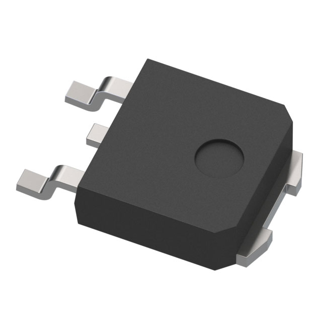
| Package Type | TO-252 (DPAK) | TO-252 (DPAK) | TO-252AA (DPAK) | — |
| Product Status | Active | Active | Active | — |
| RoHS Status | ROHS3 Compliant | ROHS3 Compliant | ROHS3 Compliant | — |
| Moisture Sensitivity Level (MSL) | 1 (Unlimited) | 1 (Unlimited) | 1 (Unlimited) | — |
Engineering Selection Recommendations
STD10NF30 (STMicroelectronics): This substitute is the primary equivalent for the AOD468 in applications requiring the full 300V voltage rating. The STD10NF30 maintains identical Vdss and package specifications while delivering 10A continuous drain current (87% of AOD468 rating) with superior on-state resistance (330mOhm vs. 420mOhm). The device carries AEC-Q101 automotive qualification, extending its suitability to automotive and industrial applications. Operating temperature range extends to -55°C, providing enhanced low-temperature performance. Gate charge increases to 23nC, requiring verification of driver circuit compatibility in high-frequency switching applications. This substitute is recommended for direct replacement in 300V applications where current demand does not exceed 10A.
FDD7N25LZTM (onsemi): This substitute operates at a reduced voltage rating of 250V Vdss and is suitable only for applications with lower voltage requirements. The device delivers 6.2A continuous drain current (54% of AOD468 rating) with higher on-state resistance (550mOhm vs. 420mOhm). The lower gate threshold voltage (2V vs. 4.5V) and reduced input capacitance (635pF vs. 790pF) provide faster switching characteristics. Operating temperature range is limited to -55 to 150°C, reducing the upper temperature margin by 25°C. This substitute is recommended only for applications with voltage requirements at or below 250V and current demands not exceeding 6.2A.
All substitutes maintain active product status, RoHS3 compliance, and unlimited moisture sensitivity level (MSL 1), ensuring regulatory conformance and long-term supply availability.
Frequently Asked Questions (FAQ)
Q: Can the STD10NF30 be used as a direct replacement for the AOD468 in all applications?
A: The STD10NF30 is a direct replacement only in applications where the continuous drain current requirement does not exceed 10A. Both devices share identical 300V Vdss rating and TO-252 package specifications. The STD10NF30 exhibits lower on-state resistance (330mOhm vs. 420mOhm), which improves efficiency. However, gate charge increases from 16nC to 23nC, requiring verification that the gate driver circuit can accommodate the higher charge without exceeding switching frequency limits.
Q: When should the FDD7N25LZTM be selected over the STD10NF30?
A: The FDD7N25LZTM is selected only when the application circuit operates at 250V or lower drain-to-source voltage. This device is not suitable for 300V applications. The FDD7N25LZTM offers faster switching characteristics due to lower gate threshold voltage (2V vs. 4.5V) and reduced input capacitance (635pF vs. 790pF). Selection of this device in 300V circuits will result in inadequate voltage margin and potential device failure.
Q: Are all three devices compatible with the same PCB layout?
A: The AOD468 and STD10NF30 use identical TO-252 (DPAK) package specifications and are mechanically compatible with the same PCB layout. The FDD7N25LZTM uses TO-252AA (DPAK) package, which maintains the same mechanical footprint and pin configuration, ensuring PCB compatibility. However, thermal performance differs due to varying power dissipation ratings (150W, 103W, and 56W respectively), which may affect thermal management design.
Q: What is the impact of higher gate charge in the STD10NF30?
A: Gate charge (Qg) of 23nC in the STD10NF30 versus 16nC in the AOD468 requires the gate driver to supply additional charge during switching transitions. This increases switching time and may increase switching losses in high-frequency applications. The gate driver circuit must be verified to deliver sufficient current to charge the gate within the required switching time window. Applications operating below 100kHz typically experience negligible impact.
Q: Do all three devices meet the same compliance and regulatory requirements?
A: All three devices are RoHS3 compliant, REACH unaffected, and classified under ECCN EAR99. All maintain unlimited moisture sensitivity level (MSL 1). The STD10NF30 carries additional AEC-Q101 automotive qualification, making it suitable for automotive applications. The AOD468 and FDD7N25LZTM do not carry automotive qualification and should not be selected for automotive applications requiring AEC-Q101 certification.
Q: What is the minimum operating temperature difference between the devices?
A: The AOD468 operates from -50°C to 175°C. Both STD10NF30 and FDD7N25LZTM extend the lower temperature limit to -55°C, providing 5°C additional margin. The FDD7N25LZTM reduces the upper temperature limit to 150°C, creating a 25°C reduction in high-temperature margin compared to the AOD468 and STD10NF30. Applications requiring operation above 150°C must use either the AOD468 or STD10NF30.
Q: How do on-state resistance differences affect power dissipation?
A: On-state resistance (Rds On) directly determines conduction losses according to the formula P = I²R. The STD10NF30 exhibits 330mOhm Rds On versus 420mOhm in the AOD468, resulting in approximately 21% lower conduction losses at equivalent current levels. The FDD7N25LZTM exhibits 550mOhm Rds On, resulting in approximately 31% higher conduction losses than the AOD468. Thermal design must account for these differences, particularly in continuous current applications.
Alternative Parts

SJ6012L2TP
Littelfuse Inc.
6 Alternative Parts

JMK107BBJ476MA-RE
Taiyo Yuden
10 Alternative Parts

GMK107BBJ475MA-T
Taiyo Yuden
5 Alternative Parts
SJ6020N2ARP
Littelfuse Inc.
3 Alternative Parts
SJ6025R2ATP
Littelfuse Inc.
4 Alternative Parts

2474-05L
API Delevan Inc.
1 Alternative Parts

4590R-684K
API Delevan Inc.
1 Alternative Parts

CM6560R-334
API Delevan Inc.
1 Alternative Parts

CM6460-104
API Delevan Inc.
1 Alternative Parts

5526-12
API Delevan Inc.
1 Alternative Parts