


Request Quote
(Ships tomorrow)
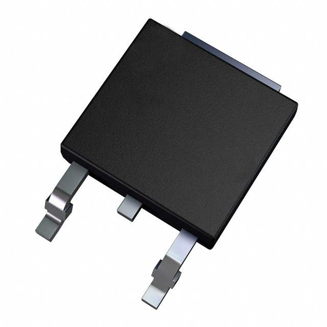
AOD458 N-Channel MOSFET 250V 14A Equivalent & Substitute Parts
Part Overview
The AOD458 is an N-Channel Metal Oxide Semiconductor Field Effect Transistor (MOSFET) manufactured by Alpha & Omega Semiconductor Inc., rated for 250V drain-to-source voltage and 14A continuous drain current. The device is housed in a Surface Mount TO-252 (DPAK) package and is designed for applications requiring moderate voltage and current switching capabilities with 150W maximum power dissipation. The AOD458 maintains Active product status and is RoHS3 compliant with unlimited moisture sensitivity level (MSL 1).
Equivalent and substitute parts are identified based on matching or exceeding critical electrical parameters including drain-to-source voltage rating, continuous drain current capability, on-state resistance characteristics, gate threshold voltage, and thermal performance specifications. Substitute devices must maintain Surface Mount DPAK packaging compatibility and equivalent or superior performance characteristics.
Substiute Parts
Key Parameters
| Parameter | Value | Unit |
|---|---|---|
| Drain to Source Voltage (Vdss) | 250 | V |
| Continuous Drain Current (Id) @ 25°C | 14 | A |
| On-State Resistance (Rds On Max) @ 7A, 10V | 280 | mOhm |
| Gate Threshold Voltage (Vgs(th) Max) @ 250µA | 4.5 | V |
| Power Dissipation (Max) | 150 | W |
| Operating Temperature Range | -50 to 175 | °C |
| Package Type | TO-252 (DPAK) | Surface Mount |
| Gate Charge (Qg Max) @ 10V | 15 | nC |
| Input Capacitance (Ciss Max) @ 25V | 770 | pF |
Substitute Part Grouping Explanation
Substitute parts for the AOD458 are qualified based on the following critical electrical and mechanical parameters:
Voltage Rating Compatibility: All substitute devices must maintain a minimum Drain-to-Source Voltage (Vdss) rating of 250V to ensure equivalent or superior voltage withstand capability.
Current Capability: Substitute devices must support a continuous drain current (Id) rating of 14A or greater at 25°C to maintain or exceed the original device's current handling capacity.
On-State Resistance (Rds On): Substitute devices must demonstrate on-state resistance characteristics that do not exceed the AOD458 specification, ensuring equivalent or improved conduction efficiency.
Package Compatibility: All substitute devices must utilize Surface Mount TO-252 (DPAK) packaging to ensure mechanical and thermal interface compatibility with existing circuit board designs.
Thermal Performance: Substitute devices must maintain adequate power dissipation ratings to support the thermal requirements of the application.
Compliance Status: All substitute devices must maintain RoHS3 compliance and equivalent regulatory certifications (REACH Unaffected, EAR99 classification).
Parameter Comparison
| Parameter | AOD458 (Main) | FQD16N25CTM | STD16NF25 | Unit |
|---|---|---|---|---|
| Manufacturer | Alpha & Omega Semiconductor Inc. | onsemi | STMicroelectronics | — |
| Drain to Source Voltage (Vdss) | 250 | 250 | 250 | V |
| Continuous Drain Current (Id) @ 25°C | 14 | 16 | 14 | A |
| On-State Resistance (Rds On Max) | 280 @ 7A, 10V | 270 @ 8A, 10V | 235 @ 6.5A, 10V | mOhm |
| Gate Threshold Voltage (Vgs(th) Max) @ 250µA | 4.5 | 4.0 | 4.0 | V |
| Gate Charge (Qg Max) @ 10V | 15 | 53.5 | 18 | nC |
| Input Capacitance (Ciss Max) @ 25V | 770 | 1080 | 680 | pF |
| Power Dissipation (Max) | 150 | 160 | 100 | W |
| Operating Temperature Range | -50 to 175 | -55 to 150 | -55 to 150 | °C |
| Package Type | TO-252 (DPAK) | TO-252AA (DPAK) | DPAK | Surface Mount |
| RoHS Status | ROHS3 Compliant | ROHS3 Compliant | ROHS3 Compliant | — |
| Product Status | Active | Active | Active | — |
Engineering Selection Recommendations
FQD16N25CTM (onsemi): This substitute device exceeds the AOD458 in continuous drain current capability (16A versus 14A) and maintains equivalent 250V voltage rating. The FQD16N25CTM demonstrates improved on-state resistance (270mOhm versus 280mOhm) and higher power dissipation rating (160W versus 150W). The device is Active status, RoHS3 compliant, and housed in TO-252AA (DPAK) packaging. The higher gate charge (53.5nC versus 15nC) and input capacitance (1080pF versus 770pF) represent trade-offs in switching speed characteristics. Operating temperature range is -55°C to 150°C, which is narrower than the AOD458 at the upper limit.
STD16NF25 (STMicroelectronics): This substitute device maintains equivalent continuous drain current (14A) and 250V voltage rating as the AOD458. The STD16NF25 demonstrates superior on-state resistance performance (235mOhm versus 280mOhm) and lower input capacitance (680pF versus 770pF). The device is Active status and RoHS3 compliant with DPAK packaging. Power dissipation rating is lower (100W versus 150W), which may limit thermal headroom in high-power applications. Gate charge is comparable (18nC versus 15nC). Operating temperature range is -55°C to 150°C, narrower than the AOD458 at the upper limit. Maximum gate voltage is ±20V versus ±30V for the AOD458.
Both substitute devices maintain Active product status and full RoHS3 compliance, ensuring regulatory and supply chain continuity. Selection between substitutes depends on application-specific requirements for current capacity, thermal performance, and switching characteristics.
Frequently Asked Questions (FAQ)
Q: Can the FQD16N25CTM directly replace the AOD458 in all applications?
A: The FQD16N25CTM is electrically compatible for applications where the AOD458 is specified, provided that the higher gate charge (53.5nC versus 15nC) and input capacitance (1080pF versus 770pF) do not negatively impact gate drive circuit performance or switching frequency requirements. The narrower upper operating temperature limit (-55°C to 150°C versus -50°C to 175°C) must be evaluated against application thermal requirements.
Q: What are the key differences between the STD16NF25 and the AOD458?
A: The STD16NF25 offers superior on-state resistance (235mOhm versus 280mOhm) and lower input capacitance (680pF versus 770pF), which may improve switching efficiency. However, the power dissipation rating is lower (100W versus 150W), and the maximum gate voltage is limited to ±20V versus ±30V. The operating temperature range is also narrower at the upper limit (150°C versus 175°C).
Q: Are all three devices housed in the same package?
A: All three devices utilize Surface Mount DPAK (TO-252) packaging with identical pin configurations and thermal interface characteristics. The AOD458 and STD16NF25 use standard TO-252-3 DPAK, while the FQD16N25CTM uses TO-252AA (DPAK), which maintains mechanical and thermal compatibility.
Q: Which substitute offers the best thermal performance?
A: The FQD16N25CTM provides the highest power dissipation rating (160W) and the highest continuous drain current capability (16A), making it suitable for applications requiring maximum thermal headroom. The STD16NF25 has a lower power dissipation rating (100W) and is better suited for moderate-power applications.
Q: Do all devices meet the same compliance standards?
A: Yes, all three devices are RoHS3 compliant, REACH Unaffected, and classified as EAR99 for export control purposes. All devices maintain Moisture Sensitivity Level 1 (Unlimited), indicating no moisture sensitivity constraints during storage or handling.
Q: What is the impact of higher gate charge on circuit design?
A: The FQD16N25CTM has significantly higher gate charge (53.5nC versus 15nC for the AOD458), which requires greater gate drive current or longer switching times. This may increase power dissipation in the gate drive circuit and reduce maximum switching frequency. The STD16NF25 has comparable gate charge (18nC), making it a closer match to the AOD458 in this parameter.
Q: Can these devices be used interchangeably in existing PCB designs?
A: Yes, all three devices are mechanically compatible with existing TO-252 (DPAK) PCB layouts. However, electrical performance differences in on-state resistance, gate charge, and input capacitance must be evaluated to ensure circuit performance remains within design specifications.
Alternative Parts

SJ6012L2TP
Littelfuse Inc.
6 Alternative Parts

JMK107BBJ476MA-RE
Taiyo Yuden
10 Alternative Parts

GMK107BBJ475MA-T
Taiyo Yuden
5 Alternative Parts
SJ6020N2ARP
Littelfuse Inc.
3 Alternative Parts
SJ6025R2ATP
Littelfuse Inc.
4 Alternative Parts

2474-05L
API Delevan Inc.
1 Alternative Parts

4590R-684K
API Delevan Inc.
1 Alternative Parts

CM6560R-334
API Delevan Inc.
1 Alternative Parts

CM6460-104
API Delevan Inc.
1 Alternative Parts

5526-12
API Delevan Inc.
1 Alternative Parts