


Request Quote
(Ships tomorrow)
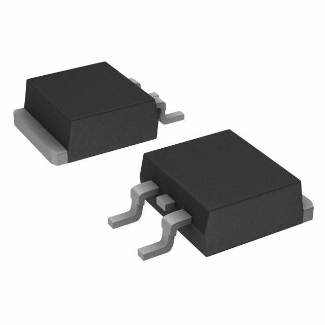
AOB411L P-Channel MOSFET 60V 8A/78A TO-263 Equivalent & Substitute Parts
Part Overview
The AOB411L is an active P-Channel MOSFET manufactured by Alpha & Omega Semiconductor Inc., rated for 60V drain-to-source voltage with continuous drain current of 8A at Ta (ambient temperature) and 78A at Tc (case temperature). The device is packaged in TO-263 (D2PAK) surface mount configuration and is ROHS3 compliant with unlimited moisture sensitivity level (MSL 1).
Substitute parts are identified when equivalent electrical performance and mechanical compatibility are required due to inventory constraints, supply chain considerations, or design flexibility within the same product category and package specification.
Substiute Parts
Key Parameters
| Parameter | Value | Unit |
|---|---|---|
| Drain-to-Source Voltage (Vdss) | 60 | V |
| Continuous Drain Current @ 25°C (Ta) | 8 | A |
| Continuous Drain Current @ 25°C (Tc) | 78 | A |
| On-State Resistance (Rds On Max) | 16.5 | mOhm @ 20A, 10V |
| Gate Threshold Voltage (Vgs(th) Max) | 2.5 | V @ 250µA |
| Gate Charge (Qg Max) | 100 | nC @ 10V |
| Input Capacitance (Ciss Max) | 6400 | pF @ 30V |
| Power Dissipation (Ta) | 2.1 | W |
| Power Dissipation (Tc) | 187 | W |
| Operating Temperature Range | -55 to 175 | °C (TJ) |
| Package Type | TO-263 (D2PAK) | Surface Mount |
| FET Type | P-Channel | MOSFET |
Substitute Part Grouping Explanation
Substitute parts for the AOB411L are qualified based on the following electrical and mechanical parameters:
Critical Matching Parameters:
- Drain-to-Source Voltage (Vdss): 60V minimum
- FET Type: P-Channel MOSFET
- Package: TO-263 (D2PAK) surface mount configuration
- Gate Voltage Rating (Vgs Max): ±20V
- Operating Temperature Range: Minimum -55°C to 175°C
Performance Equivalence Parameters:
- On-State Resistance (Rds On): Within acceptable range for the application
- Gate Threshold Voltage (Vgs(th)): Within ±0.5V tolerance
- Gate Charge (Qg): Within ±20% tolerance
- Input Capacitance (Ciss): Within ±30% tolerance
All substitute parts listed maintain identical voltage ratings, package configuration, and thermal operating range. Continuous drain current ratings may vary based on case temperature measurement conditions, but all substitutes meet or exceed the 60V Vdss specification and P-Channel MOSFET topology requirement.
Parameter Comparison
| Parameter | AOB411L (Main) | NP50P06KDG-E1-AY | SUM55P06-19L-E3 | Unit |
|---|---|---|---|---|
| Manufacturer | Alpha & Omega Semiconductor | Renesas Electronics | Vishay Siliconix | — |
| Drain-to-Source Voltage (Vdss) | 60 | 60 | 60 | V |
| FET Type | P-Channel | P-Channel | P-Channel | — |
| Continuous Drain Current (Tc) | 78 | 50 | 55 | A |
| On-State Resistance (Rds On Max) | 16.5 @ 20A, 10V | 17 @ 25A, 10V | 19 @ 30A, 10V | mOhm |
| Gate Threshold Voltage (Vgs(th) Max) | 2.5 @ 250µA | 2.5 @ 1mA | 3.0 @ 250µA | V |
| Gate Charge (Qg Max) | 100 @ 10V | 95 @ 10V | 115 @ 10V | nC |
| Input Capacitance (Ciss Max) | 6400 @ 30V | 5000 @ 10V | 3500 @ 25V | pF |
| Power Dissipation (Ta) | 2.1 | 1.8 | 3.75 | W |
| Power Dissipation (Tc) | 187 | 90 | 125 | W |
| Operating Temperature Range | -55 to 175 | Up to 175 | -55 to 175 | °C (TJ) |
| Package Type | TO-263 (D2PAK) | TO-263 (D2PAK) | TO-263 (D2PAK) | — |
| Mounting Type | Surface Mount | Surface Mount | Surface Mount | — |
| RoHS Status | ROHS3 Compliant | ROHS3 Compliant | ROHS3 Compliant | — |
| Moisture Sensitivity Level | 1 (Unlimited) | 1 (Unlimited) | 1 (Unlimited) | — |
| REACH Status | REACH Unaffected | REACH Unaffected | REACH Affected | — |
Engineering Selection Recommendations
AOB411L (Alpha & Omega Semiconductor Inc.)
- Active product status with 23,441 pieces in stock
- ROHS3 compliant and REACH unaffected
- Suitable for applications requiring the specified 60V/78A (Tc) performance envelope
- Lowest gate charge (100 nC) among the three options
NP50P06KDG-E1-AY (Renesas Electronics Corporation)
- Active product status with 4,319 pieces in stock
- ROHS3 compliant and REACH unaffected
- Continuous drain current rated at 50A (Tc), lower than AOB411L
- Lowest power dissipation at Ta (1.8W) and Tc (90W)
- Lowest input capacitance (5000 pF @ 10V)
- Suitable for applications where lower power dissipation is prioritized
SUM55P06-19L-E3 (Vishay Siliconix)
- Active product status with 16,170 pieces in stock
- ROHS3 compliant; REACH affected status requires verification for regulated applications
- Continuous drain current rated at 55A (Tc)
- TrenchFET® series technology
- Highest power dissipation capability at Tc (125W)
- Gate threshold voltage 3.0V (higher than other options)
- Suitable for applications requiring higher thermal performance
All three parts maintain identical 60V Vdss rating, P-Channel MOSFET topology, TO-263 package configuration, and ±20V gate voltage rating. Selection should be based on specific application requirements regarding continuous current handling, thermal dissipation, and regulatory compliance status.
Frequently Asked Questions (FAQ)
Q: Can the NP50P06KDG-E1-AY substitute for the AOB411L in all applications?
A: The NP50P06KDG-E1-AY is electrically compatible for applications requiring up to 50A continuous drain current at case temperature. Applications requiring the full 78A (Tc) rating of the AOB411L require verification that the lower current rating is acceptable for the specific circuit design.
Q: What is the primary difference between the three substitute options?
A: The primary differences are continuous drain current ratings (AOB411L: 78A Tc, NP50P06KDG-E1-AY: 50A Tc, SUM55P06-19L-E3: 55A Tc), power dissipation capabilities, and input capacitance values. All maintain identical 60V voltage rating and TO-263 package configuration.
Q: Are all three parts pin-compatible?
A: Yes. All three parts use the TO-263 (D2PAK) package with identical pin configuration: 2 leads plus tab. Direct PCB footprint compatibility is confirmed.
Q: Does the SUM55P06-19L-E3 REACH affected status affect its use?
A: REACH affected status indicates the part contains substances of concern under REACH regulations. Applications subject to REACH compliance requirements must evaluate whether this status is acceptable for the intended market and application.
Q: What is the significance of gate charge (Qg) differences?
A: Gate charge affects switching speed and driver circuit requirements. The AOB411L has the lowest gate charge (100 nC), which may result in faster switching characteristics compared to the NP50P06KDG-E1-AY (95 nC) and SUM55P06-19L-E3 (115 nC). Driver circuit design should account for these differences.
Q: Can input capacitance (Ciss) differences affect circuit performance?
A: Yes. Input capacitance affects gate drive requirements and switching transient behavior. The SUM55P06-19L-E3 has the lowest Ciss (3500 pF @ 25V), while the AOB411L has the highest (6400 pF @ 30V). Applications with high-frequency switching or limited gate drive capability should consider these differences.
Q: Are all parts suitable for the full -55°C to 175°C operating temperature range?
A: The AOB411L and SUM55P06-19L-E3 are specified for -55°C to 175°C. The NP50P06KDG-E1-AY is specified up to 175°C without explicit lower temperature limit documentation. Applications requiring full -55°C operation should confirm NP50P06KDG-E1-AY suitability with the manufacturer.
Q: What packaging options are available for these parts?
A: AOB411L is available in standard packaging. NP50P06KDG-E1-AY is supplied in Tape & Reel (TR) format. SUM55P06-19L-E3 is available in Cut Tape (CT) and Digi-Reel® format. All use identical TO-263 (D2PAK) component package.
Alternative Parts

SJ6012L2TP
Littelfuse Inc.
6 Alternative Parts

JMK107BBJ476MA-RE
Taiyo Yuden
10 Alternative Parts

GMK107BBJ475MA-T
Taiyo Yuden
5 Alternative Parts
SJ6020N2ARP
Littelfuse Inc.
3 Alternative Parts
SJ6025R2ATP
Littelfuse Inc.
4 Alternative Parts

2474-05L
API Delevan Inc.
1 Alternative Parts

4590R-684K
API Delevan Inc.
1 Alternative Parts

CM6560R-334
API Delevan Inc.
1 Alternative Parts

CM6460-104
API Delevan Inc.
1 Alternative Parts

5526-12
API Delevan Inc.
1 Alternative Parts