


Request Quote
(Ships tomorrow)
ADS809Y/250 Equivalent & Substitute Parts
Part Overview
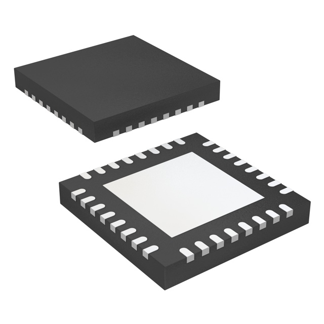
The ADS809Y/250 is a 12-bit pipelined analog-to-digital converter manufactured by Texas Instruments, designed for single-channel data acquisition applications. This device features an 80 MHz sampling rate with both differential and single-ended input capabilities, operating from a 5V supply in a 48-HTQFP package.
The ADS809Y/250 is classified as obsolete. Identifying suitable substitute components is necessary to maintain design continuity, ensure supply chain reliability, and support long-term product availability for applications currently utilizing this device.
Substiute Parts
Key Parameters
| Parameter | Value |
|---|---|
| Resolution (Bits) | 12 |
| Sampling Rate | 80 MHz |
| Number of Inputs | 1 |
| Input Type | Differential, Single Ended |
| Architecture | Pipelined |
| Data Interface | Parallel |
| Analog Supply Voltage | 5V |
| Digital Supply Voltage | 5V |
| Operating Temperature Range | -40°C to 85°C |
| Package Type | 48-HTQFP (7x7) |
| RoHS Status | ROHS3 Compliant |
Substitute Part Grouping Explanation
Substitution eligibility for the ADS809Y/250 is determined by the following core parameters:
- Resolution: 12-bit conversion capability
- Sampling Rate: 80 MHz minimum throughput
- Architecture: Pipelined ADC topology
- Data Interface: Parallel output configuration
- Reference Type: External and internal reference support
- Operating Temperature: -40°C to 85°C range
- Compliance: ROHS3 and REACH compliance status
The ADC12C080CISQE/NOPB qualifies as a manufacturer-recommended substitute based on matching these core electrical specifications. While the package format differs (32-WQFN versus 48-HTQFP), the functional performance parameters remain equivalent, and the substitute maintains active product status with current manufacturing support.
Parameter Comparison
| Parameter | ADS809Y/250 | ADC12C080CISQE/NOPB | Match Status |
|---|---|---|---|
| Manufacturer | Texas Instruments | Texas Instruments | Match |
| Resolution (Bits) | 12 | 12 | Match |
| Sampling Rate (MHz) | 80 | 80 | Match |
| Number of Inputs | 1 | 1 | Match |
| Architecture | Pipelined | Pipelined | Match |
| Data Interface | Parallel | Parallel | Match |
| Reference Type | External, Internal | External, Internal | Match |
| Operating Temperature | -40°C to 85°C | -40°C to 85°C | Match |
| Input Type | Differential, Single Ended | Differential | Partial |
| Analog Supply Voltage | 5V | 2.7V to 3.6V | Different |
| Digital Supply Voltage | 5V | 2.4V to 3.6V | Different |
| Package Type | 48-HTQFP (7x7) | 32-WQFN (5x5) | Different |
| Product Status | Obsolete | Active | Substitute Advantage |
| RoHS Status | ROHS3 Compliant | ROHS3 Compliant | Match |
Engineering Selection Recommendations
The ADC12C080CISQE/NOPB is the manufacturer-recommended substitute for the obsolete ADS809Y/250. This recommendation is based on:
Product Status: The ADC12C080CISQE/NOPB maintains active manufacturing status, ensuring long-term availability and supply chain continuity compared to the obsolete ADS809Y/250.
Electrical Equivalence: Both devices share identical 12-bit resolution, 80 MHz sampling rate, pipelined architecture, and parallel data interface specifications. The core data acquisition functionality is preserved.
Compliance Alignment: Both parts maintain ROHS3 compliance and REACH unaffected status, meeting regulatory requirements for equivalent component substitution.
Design Considerations: The substitute operates at lower supply voltages (2.7V to 3.6V analog, 2.4V to 3.6V digital) compared to the original 5V requirement. This represents a functional improvement for modern low-power applications but requires circuit redesign for existing 5V systems. The package transition from 48-HTQFP to 32-WQFN (5x5) reduces board footprint and requires PCB layout modification. The substitute supports differential input only, whereas the original supported both differential and single-ended configurations.
Frequently Asked Questions (FAQ)
Q: Can the ADC12C080CISQE/NOPB directly replace the ADS809Y/250 without circuit modifications?
A: Direct pin-for-pin replacement is not possible due to different package formats (48-HTQFP versus 32-WQFN) and supply voltage requirements (5V versus 2.7V–3.6V). PCB layout redesign and power supply circuit modification are required.
Q: What are the key electrical differences between these devices?
A: The core data acquisition parameters—12-bit resolution, 80 MHz sampling rate, pipelined architecture, and parallel interface—are identical. The primary differences are supply voltage ranges and input type support. The ADC12C080CISQE/NOPB operates at lower voltages and supports differential input only, whereas the ADS809Y/250 supports both differential and single-ended inputs.
Q: Is the ADC12C080CISQE/NOPB suitable for applications requiring single-ended input?
A: No. The ADC12C080CISQE/NOPB supports differential input only. Applications requiring single-ended input capability must evaluate alternative substitutes or retain the original ADS809Y/250 if available.
Q: What is the impact of the package change from 48-HTQFP to 32-WQFN?
A: The 32-WQFN package is smaller (5x5 mm versus 7x7 mm) and reduces board footprint. However, this requires complete PCB layout redesign, including trace routing, via placement, and thermal management considerations. The pin count reduction from 48 to 32 indicates functional consolidation in the newer design.
Q: Are both devices RoHS and REACH compliant?
A: Yes. Both the ADS809Y/250 and ADC12C080CISQE/NOPB are ROHS3 compliant and REACH unaffected, meeting regulatory requirements for equivalent component substitution.
Q: Why is the ADC12C080CISQE/NOPB recommended despite supply voltage differences?
A: The manufacturer recommendation is based on functional equivalence in core data acquisition specifications and active product status. The lower supply voltage requirement represents a design improvement for modern applications. However, existing 5V systems require power supply circuit redesign to utilize this substitute.
Alternative Parts

SJ6012L2TP
Littelfuse Inc.
6 Alternative Parts

JMK107BBJ476MA-RE
Taiyo Yuden
10 Alternative Parts

GMK107BBJ475MA-T
Taiyo Yuden
5 Alternative Parts
SJ6020N2ARP
Littelfuse Inc.
3 Alternative Parts
SJ6025R2ATP
Littelfuse Inc.
4 Alternative Parts

2474-05L
API Delevan Inc.
1 Alternative Parts

4590R-684K
API Delevan Inc.
1 Alternative Parts

CM6560R-334
API Delevan Inc.
1 Alternative Parts

CM6460-104
API Delevan Inc.
1 Alternative Parts

5526-12
API Delevan Inc.
1 Alternative Parts