


Request Quote
(Ships tomorrow)
AD744KNZ Equivalent & Substitute Parts
Part Overview
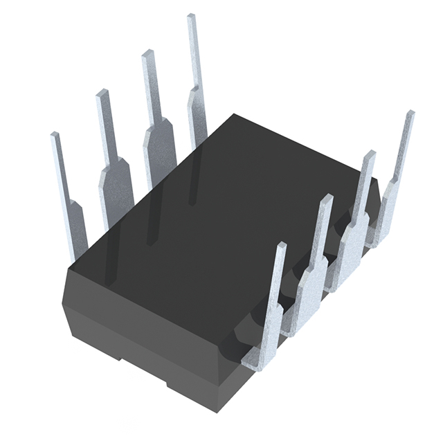
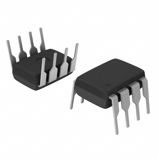
The AD744KNZ is a J-FET input operational amplifier manufactured by Analog Devices Inc., housed in an 8-DIP through-hole package. This linear amplifier circuit is designed for applications requiring low input bias current and low input offset voltage characteristics. The device is currently in active production status with 1529 units available in stock.
Substitute parts are identified based on matching functional category, package type, mounting configuration, and critical electrical parameters. Alternative components may be required due to inventory constraints, design optimization, or application-specific performance requirements.
Substiute Parts
Key Parameters
| Parameter | Value | Unit |
|---|---|---|
| Amplifier Type | J-FET | — |
| Number of Circuits | 1 | — |
| Slew Rate | 75 | V/µs |
| -3dB Bandwidth | 13 | MHz |
| Current - Input Bias | 30 | pA |
| Voltage - Input Offset | 250 | µV |
| Current - Supply | 3.5 | mA |
| Current - Output / Channel | 25 | mA |
| Voltage - Supply Span (Min) | 9 | V |
| Voltage - Supply Span (Max) | 36 | V |
| Operating Temperature | 0 to 70 | °C |
| Package / Case | 8-DIP (0.300", 7.62mm) | — |
| Mounting Type | Through Hole | — |
| RoHS Status | ROHS3 Compliant | — |
| Moisture Sensitivity Level | 1 (Unlimited) | — |
Substitute Part Grouping Explanation
Substitute parts for the AD744KNZ are selected based on the following criteria:
Primary Matching Parameters:
- Package type: 8-DIP (0.300", 7.62mm) through-hole configuration
- Mounting type: Through-hole
- Number of circuits: Single circuit per package
- Supply voltage range compatibility: Minimum 9 V to maximum 36 V
- Compliance certifications: ROHS3 Compliant, REACH Unaffected, EAR99 classification
Secondary Electrical Compatibility:
- Slew rate: 75 V/µs or greater
- Bandwidth: 13 MHz or greater
- Input bias current: 30 pA or lower
- Input offset voltage: 250 µV or lower
- Output current capability: 25 mA or greater
- Supply current: Within acceptable operating range
The identified substitutes maintain functional equivalence within the linear amplifier category while meeting the specified electrical and mechanical constraints.
Parameter Comparison
| Parameter | AD744KNZ | LT1122CCN8#PBF | OPA627AP | Unit |
|---|---|---|---|---|
| Manufacturer | Analog Devices Inc. | Analog Devices Inc. | Texas Instruments | — |
| Amplifier Type | J-FET | J-FET | General Purpose | — |
| Number of Circuits | 1 | 1 | 1 | — |
| Slew Rate | 75 | 75 | 55 | V/µs |
| Bandwidth / Gain Bandwidth Product | 13 | 13 | 16 | MHz |
| Current - Input Bias | 30 | 12 | 2 | pA |
| Voltage - Input Offset | 250 | 130 | 130 | µV |
| Current - Supply | 3.5 | 7.8 | 7 | mA |
| Current - Output / Channel | 25 | — | 45 | mA |
| Voltage - Supply Span (Min) | 9 | 10 | 9 | V |
| Voltage - Supply Span (Max) | 36 | 36 | 36 | V |
| Operating Temperature | 0 to 70 | -40 to 85 | -25 to 85 | °C |
| Package / Case | 8-DIP (0.300", 7.62mm) | 8-DIP (0.300", 7.62mm) | 8-DIP (0.300", 7.62mm) | — |
| Mounting Type | Through Hole | Through Hole | Through Hole | — |
| Product Status | Active | Active | Obsolete | — |
| RoHS Status | ROHS3 Compliant | ROHS3 Compliant | ROHS3 Compliant | — |
| Moisture Sensitivity Level | 1 (Unlimited) | 1 (Unlimited) | 1 (Unlimited) | — |
Engineering Selection Recommendations
LT1122CCN8#PBF (Analog Devices Inc.)
The LT1122CCN8#PBF is an active production substitute with identical package configuration and slew rate specification. This device offers improved input bias current (12 pA versus 30 pA) and lower input offset voltage (130 µV versus 250 µV). The extended operating temperature range (-40°C to 85°C) provides broader environmental coverage compared to the AD744KNZ. Supply voltage compatibility spans 10 V to 36 V, with the minimum threshold 1 V higher than the primary part. All compliance certifications match the AD744KNZ specification. Higher supply current consumption (7.8 mA versus 3.5 mA) must be evaluated within the application power budget.
OPA627AP (Texas Instruments)
The OPA627AP is classified as obsolete product status and should be selected only when inventory of active alternatives is unavailable. This device features a general-purpose amplifier topology rather than J-FET input architecture. The OPA627AP provides superior input bias current (2 pA) and higher output current capability (45 mA versus 25 mA). Slew rate is reduced to 55 V/µs, and bandwidth is increased to 16 MHz. Operating temperature range extends to -25°C to 85°C. All compliance certifications are equivalent to the primary part. The obsolete status and different amplifier topology present long-term supply and performance consistency risks.
Frequently Asked Questions (FAQ)
Q: Can the LT1122CCN8#PBF be used as a direct replacement for the AD744KNZ?
A: The LT1122CCN8#PBF shares identical package configuration (8-DIP through-hole), slew rate (75 V/µs), and bandwidth (13 MHz). Both devices are J-FET input amplifiers with active production status and ROHS3 compliance. The LT1122CCN8#PBF operates at a higher minimum supply voltage (10 V versus 9 V) and consumes greater supply current (7.8 mA versus 3.5 mA). Pin-level compatibility must be verified against the specific application schematic.
Q: What are the key differences between the AD744KNZ and OPA627AP?
A: The OPA627AP uses general-purpose amplifier topology rather than J-FET input design. Input bias current is significantly lower (2 pA versus 30 pA), and output current capability is higher (45 mA versus 25 mA). Slew rate is reduced to 55 V/µs. The OPA627AP is classified as obsolete, whereas the AD744KNZ is in active production. Both devices use identical 8-DIP through-hole packaging.
Q: Are all substitute parts ROHS3 compliant?
A: Yes. The AD744KNZ, LT1122CCN8#PBF, and OPA627AP are all ROHS3 compliant with moisture sensitivity level 1 (unlimited). All three devices are REACH unaffected and classified as EAR99 for export control purposes.
Q: What is the impact of supply voltage differences between substitutes?
A: The AD744KNZ operates from 9 V to 36 V. The LT1122CCN8#PBF requires a minimum of 10 V, which may restrict operation in applications using 9 V single-supply configurations. The OPA627AP operates from 9 V to 36 V, matching the primary part specification. Maximum supply voltage is 36 V for all three devices.
Q: How do input offset voltage specifications compare?
A: The AD744KNZ specifies 250 µV input offset voltage. The LT1122CCN8#PBF and OPA627AP both specify 130 µV, representing a 48% reduction. Lower input offset voltage reduces DC error in precision signal conditioning applications. Offset voltage drift with temperature must be evaluated separately from the static specification.
Q: Can the OPA627AP be used in new designs?
A: The OPA627AP is classified as obsolete product status. While functional equivalence exists for the 8-DIP package and general electrical parameters, obsolete classification indicates discontinued manufacturing and limited future availability. New designs should prioritize active production alternatives such as the LT1122CCN8#PBF or AD744KNZ.
Q: What mounting considerations apply to all substitute parts?
A: All three devices use through-hole mounting in 8-DIP (0.300", 7.62mm) package configuration. Pin spacing, lead diameter, and insertion depth are identical across all substitutes. PCB footprint compatibility is maintained for direct socket replacement without layout modification.
Alternative Parts

SJ6012L2TP
Littelfuse Inc.
6 Alternative Parts

JMK107BBJ476MA-RE
Taiyo Yuden
10 Alternative Parts

GMK107BBJ475MA-T
Taiyo Yuden
5 Alternative Parts
SJ6020N2ARP
Littelfuse Inc.
3 Alternative Parts
SJ6025R2ATP
Littelfuse Inc.
4 Alternative Parts

2474-05L
API Delevan Inc.
1 Alternative Parts

4590R-684K
API Delevan Inc.
1 Alternative Parts

CM6560R-334
API Delevan Inc.
1 Alternative Parts

CM6460-104
API Delevan Inc.
1 Alternative Parts

5526-12
API Delevan Inc.
1 Alternative Parts