


Request Quote
(Ships tomorrow)
9DBU0741AKLF Equivalent & Substitute Parts
Part Overview
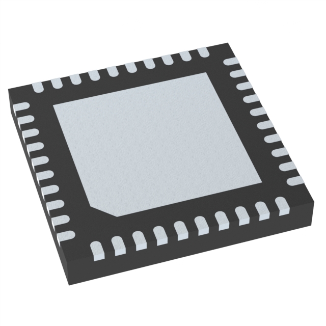
The 9DBU0741AKLF is a PCI Express (PCIe) buffer IC manufactured by Renesas Electronics Corporation, designed to distribute clock signals with 1 output at 167MHz maximum frequency. This device operates at 1.425V to 1.575V supply voltage and is housed in a 40-VFQFN (5x5) package with exposed pad. The part is classified as obsolete, making identification of suitable substitute components essential for ongoing system support and new design implementations.
Substiute Parts
Key Parameters
| Parameter | Value |
|---|---|
| Manufacturer Part Number | 9DBU0741AKLF |
| Manufacturer | Renesas Electronics Corporation |
| Category | Clock/Timing |
| Main Purpose | PCI Express (PCIe) |
| Frequency - Max | 167MHz |
| Input Type | HCSL |
| Output Type | LP-HCSL |
| Number of Circuits | 1 |
| Ratio - Input:Output | 1:7 |
| Differential - Input:Output | Yes/Yes |
| Voltage - Supply | 1.425V ~ 1.575V |
| Operating Temperature | 0°C ~ 70°C |
| Package / Case | 40-VFQFN Exposed Pad |
| Mounting Type | Surface Mount |
| Product Status | Obsolete |
| RoHS Status | ROHS3 Compliant |
| Moisture Sensitivity Level (MSL) | 3 (168 Hours) |
Substitute Part Grouping Explanation
Substitution of the 9DBU0741AKLF is determined by the following critical parameters:
Package Compatibility: Both the main part and substitute must use the 40-VFQFN (5x5) Exposed Pad package to ensure PCB layout compatibility and mounting feasibility.
Functional Category: Both parts must serve PCI Express (PCIe) clock distribution applications with differential input and output signaling (HCSL/LP-HCSL).
Differential Signaling: Input and output must both support differential signal transmission to maintain signal integrity in PCIe applications.
Surface Mount Technology: Both parts must be surface-mount devices compatible with standard assembly processes.
Compliance Standards: Both parts must maintain ROHS3 compliance and equivalent moisture sensitivity ratings to ensure environmental and regulatory compatibility.
The RC19008A100GND#BB0 qualifies as a substitute based on these parameters, though with notable differences in maximum frequency, supply voltage range, and output ratio that must be evaluated for specific application requirements.
Parameter Comparison
| Parameter | 9DBU0741AKLF | RC19008A100GND#BB0 |
|---|---|---|
| Manufacturer | Renesas Electronics Corporation | Renesas Electronics Corporation |
| Category | Clock/Timing | Clock/Timing |
| Main Purpose | PCI Express (PCIe) | PCI Express (PCIe) |
| Input Type | HCSL | HCSL, LVDS |
| Output Type | LP-HCSL | LP-HCSL |
| Number of Circuits | 1 | 1 |
| Ratio - Input:Output | 1:7 | 1:8 |
| Differential - Input:Output | Yes/Yes | Yes/Yes |
| Frequency - Max | 167MHz | 400MHz |
| Voltage - Supply | 1.425V ~ 1.575V | 2.97V ~ 3.63V |
| Operating Temperature | 0°C ~ 70°C | -40°C ~ 105°C (TA) |
| Package / Case | 40-VFQFN Exposed Pad | 40-VFQFN Exposed Pad |
| Mounting Type | Surface Mount | Surface Mount |
| Product Status | Obsolete | Active |
| RoHS Status | ROHS3 Compliant | ROHS3 Compliant |
| Moisture Sensitivity Level (MSL) | 3 (168 Hours) | 3 (168 Hours) |
Engineering Selection Recommendations
The RC19008A100GND#BB0 is available as an active product from Renesas Electronics Corporation, providing supply continuity for applications currently using the obsolete 9DBU0741AKLF. Both devices maintain identical ROHS3 compliance and MSL ratings, ensuring equivalent environmental and regulatory standing.
Selection of the RC19008A100GND#BB0 requires evaluation of the following differences:
Supply Voltage: The substitute operates at 2.97V to 3.63V, compared to the main part's 1.425V to 1.575V. Power supply architecture must be adjusted accordingly.
Maximum Frequency: The substitute supports 400MHz operation versus 167MHz for the main part, providing enhanced frequency capability for future-generation PCIe implementations.
Output Ratio: The substitute provides 1:8 output distribution compared to 1:7 for the main part, resulting in one additional output channel.
Operating Temperature Range: The substitute extends the operating range to -40°C to 105°C, compared to 0°C to 70°C for the main part, enabling broader environmental deployment.
Input Compatibility: The substitute accepts both HCSL and LVDS inputs, providing greater input signal flexibility compared to HCSL-only input on the main part.
Frequently Asked Questions (FAQ)
Q: Can the RC19008A100GND#BB0 directly replace the 9DBU0741AKLF without PCB modifications?
A: Both devices use the identical 40-VFQFN (5x5) Exposed Pad package, allowing direct footprint compatibility. However, power supply voltage requirements differ significantly (1.425V–1.575V versus 2.97V–3.63V), necessitating power delivery circuit modifications.
Q: What is the significance of the 1:7 versus 1:8 output ratio difference?
A: The main part provides 7 differential output pairs from a single differential input. The substitute provides 8 output pairs. Applications requiring exactly 7 outputs must either leave one output unused or redesign the signal distribution architecture.
Q: Are both parts suitable for new PCIe Gen 3 designs?
A: The 9DBU0741AKLF is obsolete and unsuitable for new designs. The RC19008A100GND#BB0 is active and supports higher frequency operation (400MHz), making it appropriate for current PCIe implementations.
Q: Do both parts require identical PCB layout considerations?
A: Both parts use the same package and differential signaling architecture, so core layout principles remain consistent. However, the substitute's higher maximum frequency may require more stringent trace impedance control and signal integrity analysis.
Q: What is the impact of the extended operating temperature range on system design?
A: The substitute's -40°C to 105°C range versus the main part's 0°C to 70°C allows deployment in industrial and automotive environments. Applications limited to commercial temperature ranges (0°C–70°C) do not require this extended capability.
Alternative Parts

SJ6012L2TP
Littelfuse Inc.
6 Alternative Parts

JMK107BBJ476MA-RE
Taiyo Yuden
10 Alternative Parts

GMK107BBJ475MA-T
Taiyo Yuden
5 Alternative Parts
SJ6020N2ARP
Littelfuse Inc.
3 Alternative Parts
SJ6025R2ATP
Littelfuse Inc.
4 Alternative Parts

2474-05L
API Delevan Inc.
1 Alternative Parts

4590R-684K
API Delevan Inc.
1 Alternative Parts

CM6560R-334
API Delevan Inc.
1 Alternative Parts

CM6460-104
API Delevan Inc.
1 Alternative Parts

5526-12
API Delevan Inc.
1 Alternative Parts